DATAMATH CALCULATOR MUSEUM
|
|
DATAMATH CALCULATOR MUSEUM |
 Both Engineering and Marketing teams obviously like fancy buzzword-abbreviations and these and some others apply to Texas Instruments’ Calculator History started in 1958 with the
Invention of the Integrated Circuit (IC) and the
Cal-Tech program in 1965 that led to the development of the World’s first battery powered Electronic Calculator, commercialized by Canon with the famous
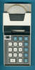
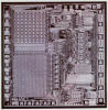
Pocketronic introduced in April 1970. The main electronics of the Pocketronic makes use of three Integrated Circuits to scan the keyboard, perform calculations and control the printer mechanism to visualize the entries and result. These
customized chips with part numbers TMC1730, TMC1731, and TMC1732 were manufactured in a "state of the art" 10-micron 1-metal PMOS process and using Dual-Inline Ceramic or Plastic (DIC/DIP) packages with 40 pins and 28 pins. TMC in the part number is for Texas Instruments, metal–oxide–semiconductor (MOS) process, Custom design.
Both Engineering and Marketing teams obviously like fancy buzzword-abbreviations and these and some others apply to Texas Instruments’ Calculator History started in 1958 with the
Invention of the Integrated Circuit (IC) and the
Cal-Tech program in 1965 that led to the development of the World’s first battery powered Electronic Calculator, commercialized by Canon with the famous
Pocketronic introduced in April 1970. The main electronics of the Pocketronic makes use of three Integrated Circuits to scan the keyboard, perform calculations and control the printer mechanism to visualize the entries and result. These
customized chips with part numbers TMC1730, TMC1731, and TMC1732 were manufactured in a "state of the art" 10-micron 1-metal PMOS process and using Dual-Inline Ceramic or Plastic (DIC/DIP) packages with 40 pins and 28 pins. TMC in the part number is for Texas Instruments, metal–oxide–semiconductor (MOS) process, Custom design.
 Nippon Calculating Machine Corporation of Japan, better known as Busicom Corporation, went during the development of their printing desktop calculator 141-PF starting in 1968 a different path and charged Intel with the development of the main electronics based on “building blocks” instead of customized chips, differing only in the “program” stored in ROM (Read-only-Memory). By November 1971 the first commercially available Microprocessor, aka Intel
i4004 Central Processing Unit (CPU) was introduced together with three more Integrated Circuits forming a complete Micro Computing System:
Nippon Calculating Machine Corporation of Japan, better known as Busicom Corporation, went during the development of their printing desktop calculator 141-PF starting in 1968 a different path and charged Intel with the development of the main electronics based on “building blocks” instead of customized chips, differing only in the “program” stored in ROM (Read-only-Memory). By November 1971 the first commercially available Microprocessor, aka Intel
i4004 Central Processing Unit (CPU) was introduced together with three more Integrated Circuits forming a complete Micro Computing System:
|
• i4001, 256 x 8 bits Mask-Programmable Read-only Memory (Mask ROM) with a 4-bit programmable I/O port • i4002, 320-bit Random-access Memory (RAM) and 4-bit output port • i4003, 10-bit shift register • i4004, 4-bit Central Processing Unit (CPU), the Microprocessor, with a maximum clock speed of 750 kHz |
The Busicom 141-PF used for its main electronics actually:
|
• 4 * i4001 for 1,024 x 8 bits Mask ROM or 1k Bytes (!) and 16 Input/Output lines • 2 * i4002 for 640 bits RAM or 80 Bytes and 8 Output lines • 3 * i4003 for 30 bits Register Memory or Processor Registers for calculations • 1 * i4004 4-bit CPU with a maximum clock speed of 750 kHz |
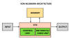 The computer architecture chosen by Intel is known as “von Neumann architecture”, named after John von Neumann, a Hungarian-American mathematician, and based on four main components:
|
• A processing unit that contains an Arithmetic Logic Unit (ALU) and Processor Registers • A control unit that contains an Instruction Register (IR) and Program Counter (PC) • Memory that stores data and instructions • Input and output mechanisms |
Bottle-neck of the von Neumann architecture is the shared memory bus used for both data and program (instructions) memory, advantage is its simplicity using Memory-mapped Input/Output devices and hence allowing very compact designs of Microcontroller Units (MCU), better known as Microcontrollers.
 Back to Texas Instruments, back to Calculators. When Gary Boone started working on a “computer-on-a-chip”, not only the TMS100 (or TMS0100) single-chip calculator used with the famous Bowmar
901B was born, but its offspring TMS1000 (used first with TI’s
SR-16) was introduced as the first commercial available Microcomputer and the U.S. Patent and Trademark Office has affirmed that Texas Instruments engineer Gary W. Boone is the inventor of the single-chip microcontroller, a device that revolutionized electronics by putting all the functions of a computer on one piece of silicon.
Back to Texas Instruments, back to Calculators. When Gary Boone started working on a “computer-on-a-chip”, not only the TMS100 (or TMS0100) single-chip calculator used with the famous Bowmar
901B was born, but its offspring TMS1000 (used first with TI’s
SR-16) was introduced as the first commercial available Microcomputer and the U.S. Patent and Trademark Office has affirmed that Texas Instruments engineer Gary W. Boone is the inventor of the single-chip microcontroller, a device that revolutionized electronics by putting all the functions of a computer on one piece of silicon.
Looking into the specifications of the TMS1802, the first commercially available member of the then new TMS100 (or TMS0100) family, reveals:
|
• 3,520 bits or 320 words of 11-bit Mask ROM (about 440 Bytes) • 182 bits (3 Registers * 13 digits, 2 * 13 bit flags) of Register Memory (about 20 Bytes) • 19 Output lines for up to 11 digits 7-Segment LED displays • 4 Input lines to scan keyboard matrices of up to 44 keys • 4-bit CPU with a maximum clock speed of 300 kHz |
Comparing these figures of the first MPU used with the Bowmar 901B and the main electronics of the Busicom 141-PF, composed of 10 Integrated Circuits centered around an i4004 MCU – brings our attention to Moore’s Law:
In 1965, Gordon E. Moore - co-founder of Intel - postulated that the number of transistors that can be packed into a given unit of space will double about every two years.
Both Bowmar 901B and Busicom 141-PF use very similar technology from Fall 1971, with the MCU based architecture sporting about 5 times the performance of the MPU based architecture. But keep in mind: 10 Integrated Circuits vs. a Single-Chip design!
Consequently there is always a Ping Pong game going back and forth:
|
• Introduce new features with complex technology and high costs • Use Moore’s Law to apply higher integration over time and hence reducing complexity and costs • Introduce new features Rinse and repeat |
This cycle applies perfectly to Graphing Calculators and ASICs (Application Specific Integrated Circuits) are an important part of it.
ASIC: An ASIC is an Integrated Circuit (IC) customized for a particular use, rather than intended for general-purpose use.
Gate Array: Early ASICs used Gate Arrays, prefabricated chips with transistors that are later interconnected into logic devices like Gates and Registers according to a custom order by adding metal interconnect layers in the factory. Customization occurred by varying a metal interconnect mask. Gate arrays had complexities of up to a few thousand gates.
Standard-cell Designs: Standard cells use a higher abstraction level of Gate Arrays, rather complex building blocks like an Adder or even a complete CPU are already predefined by the ASIC manufacturer instead of designed and engineered from scratch by the customer.
System-on-Chip (SOC): A System-on-Chip is an IC that integrates most components of a computer or other electronic system, typically using a CPU, Memory, Input/Output ports and secondary storage. It must contain digital, analog, mixed-signal, or radio frequency signal processing functions, otherwise it will only be considered as an application specific processor.
Application-specific Standard Product (ASSP): An Application-specific Standard Product or ASSP is an IC that implements a specific function that appeals to a wide market. As opposed to ASICs that combine a collection of functions and are designed by or for one customer, ASSPs are available as off-the-shelf components and typically customized by software only.
Texas Instruments entered the market of Graphing calculators in 1990 with the TI-81 based on Toshiba T6A49A Application-specific 8-bit Z80 CPU, 128k Bytes Mask ROM, 8k Bytes Static RAM (SRAM) and three display drivers from Toshiba for the 64 * 96 pixel dot matrix LC-Display. This basic architecture branched into three product lines before being replaced in 1999 by the TI-83 Plus architecture using more flexible Flash ROM instead the Mask ROM:
|
• 1990:
TI-81,
TI-82, TI-83,
TI-82 STATS • 1992: TI-85, TI-86 • 1995: TI-80 |
Interesting to notice that Texas Instruments switched back and forth between ASSP and CPU + ASIC based solutions:
| Product | Intro. | Date Code | CPU/ASSP | ASIC | RAM (Bytes) |
ROM (Bytes) |
Display (Pixel) |
Driver | Comments |
| TI-81 | 1990 | (I-0490) | Toshiba T6A49 |
8k | 64k ©1990 |
64 * 96 | 2 * T7778A, T7900 | Engineering Sample | |
| May 1990 |
I-0990 | Toshiba T6A49A |
8k | 64k ©1990 |
64 * 96 | 2 * T7778A, T7900 | no backup battery | ||
| March 1991 |
I-0991 | Toshiba T6A43 |
8k | 64k ©1991 |
64 * 96 | 2 * T7778A, T7900 | no backup battery | ||
| March 1992 |
I-1192B | Toshiba T6A43 |
8k | 64k ©1991 |
64 * 96 | 2 * T6A39, T6A40 | backup battery | ||
| October 1993 |
I-0894F | Toshiba T84C00A |
Toshiba TC14L010 |
8k | 64k ©1993 |
64 * 96 | T6A04 | backup battery | |
| TI-82 | (August 1993) |
(I-0693) | Toshiba T84C00A |
Toshiba TC14L010 |
32k | 128k OTP |
64 * 96 | T6A04 | Engineering Sample |
| August 1993 |
I-0194K | Toshiba T84C00A |
Toshiba TC14L010 |
32k | 128k ©1993 |
64 * 96 | T6A04 | ||
| January 1995 |
I-1295A | Toshiba T84C00A |
Toshiba TC14L010 |
32k | 128k ©1995 |
64 * 96 | T6A04 | ||
| March 1999 |
I-0200U | Zilog Z84C0008 |
Toshiba TC14L010 |
32k | 128k ©1995 |
64 * 96 | T6A04A | New design | |
| June 2000 |
S-0803A | Toshiba T6C79 |
32k | 128k ©2000 |
64 * 96 | T6A04A | Parcus | ||
| TI-82 STATS | July 2004 |
S-0304B | Toshiba T6C79 |
32k | 128k ©2004 |
64 * 96 | T6A04A | ||
| TI-83 | January 1996 |
I-0496A | Toshiba T84C00A |
Toshiba TC14L010 |
32k | 256k OTP |
64 * 96 | T6A04 | |
| January 1996 |
I-0597H | Toshiba T6C79 |
32k | 256k ©1996 |
64 * 96 | T6A04 | |||
| (March 1999) |
(I-0598) | Toshiba T6C79 |
32k | 256k ©1998 |
64 * 96 | T6A04 | Engineering Sample | ||
| March 1999 |
I-1099N | Toshiba T6C79 |
32k | 256k ©1998 |
64 * 96 | T6A04A | New design | ||
| June 2000 |
I-0700A | Toshiba T6C79 |
32k | 256k ©2000 |
64 * 96 | T6A04A | Parcus | ||
| TI-85 | March 1992 |
I-1092 | Toshiba T6A43 |
32k | 128k OTP |
64 * 128 | 2 * T6A39, T6A40 | ||
| January 1995 |
I-0395G | Toshiba T6A43 |
32k | 128k ©1993 |
64 * 128 | 2 * T6A39, T6A40 | |||
| TI-86 | May 1997 |
(I-0297) | Toshiba T6A43 |
128k | 256k OTP |
64 * 128 | T6A23, T6A40 | Engineering Sample | |
| May 1997 |
I-1197E | Toshiba T6A43 |
128k | 256k OTP |
64 * 128 | T6A23, T6A40 | |||
| May 1997 |
I-0400K | Toshiba T6A43 |
128k | 256k ©1998 |
64 * 128 | T6A23, T6A40 | |||
| TI-80 | February 1995 |
I-1296C | Toshiba T6M53A |
8k | 64k ©1995 |
48 * 64 | T6B79 |
Mask ROM was in the Eighties and Nineties of the last Century in high quantities a very economical solution as program memory for Graphing calculators but had three main disadvantages:
|
• Very high non-recurring engineering (NRE) cost or one-time cost to manufacture a Mask ROM • Very long lead time to change the Mask ROM in case of program bugs or new features • No “field-programmability” to modify the program "in the field," without disassembling the calculator or returning it to its manufacturer |
Recognizing about 13 different software versions for the TI-82 alone, obviously a change was needed and Texas Instruments introduced in 1998 with the TI-73 a groundbreaking architecture based on Flash ROM technology that was adopted in 1999 for the TI-83 Plus. Flash ROM technology is allowing users not only to download and install numerous software applications and additional functionality beyond math and science to their Graphing calculators, but even download the latest software version (Operating System). These reasons and more have made the TI-83 Plus the best-selling Graphing calculator in the US and Canada. In the year 2000 more than 2,000,000 units were shipped! Already on July 22, 2003 reported Texas Instruments an accumulated shipment of 25,000,000 Graphing calculators since the introduction of the TI-81.
From a technical point of view is the first generation of the TI-83 Plus very similar to the TI-82 with greatly enhanced memory capacity using an 8-bit Z80 CPU with an ASIC for its glue logic, 512k Bytes Flash ROM, 32k Bytes Static RAM (SRAM) and one display driver from Toshiba for the 64 * 96 pixel dot matrix LC-Display. The longevity of the TI-83 Plus architecture led due to Moore’s Law to another major topic: End-of-life (EOL) of critical products like ASICs supplied to Texas Instruments and their OEMs, indicating that the product is in the end of its useful life (from the vendor's point of view), and a vendor stops marketing, selling, or rework sustaining it. Moore’s Law is based on the improvements in chip manufacturing technology and doubling the number of transistors packed into an IC every two years translates into frequent process changes. A manufacturer of ICs is usually not able running too many manufacturing processes in parallel and hence will discontinue ICs based on mature processes from time to time. Therefore you’ll notice various technologies used with this Graphing calculator architecture. Learn more about the seven known TI-83 Plus Hardware Versions introduced between 1999 and 2007.
The basic architecture branched between 1999 and 2015 into 2 design lines covering multiple products:
Product Overview:
| Product | Intro. | Date Code | CPU/ASSP | ASIC | RAM (Bytes) |
ROM (Bytes) |
Display (Pixel) |
Driver | Comments |
| TI-73 TI-73 Explorer |
March 1998 |
I-0199 | Zilog Z84C0008 |
TI REF 9815455 |
32k | 512k Flash |
64 * 96 | Toshiba T6A04 |
|
| March 2003 |
S-0404D | Zilog Z84C0008 |
TI REF 9815455 |
32k | 512k Flash |
64 * 96 | Toshiba T6A04A |
||
| July 2006 |
S-0307F | TI REF TI-738X |
ASSP 32k |
512k Flash |
64 * 96 | Novatek NT7564H |
|||
| July 2006 |
P-0308G | TI REF TI-738X |
ASSP 32k |
512k Flash |
64 * 96 | Toshiba T6A04A |
|||
| January 2009 |
P-1108I | TI REF TI-738X |
ASSP 32k |
512k Flash |
64 * 96 | Novatek NT7564H |
TI-84 housing | ||
| TI-Lycée Pro.fr TI-76.fr |
(June 2009) |
(P-0708) | TI REF TI-738X |
ASSP 32k |
512k Flash |
64 * 96 | Toshiba T6K04 |
||
| June 2009 |
P-0409 | TI REF TI-738X |
ASSP 32k |
512k Flash |
64 * 96 | Novatek NT7564H |
|||
| TI-82 Stats.fr TI-82 STATS |
July 2006 |
S-0606F | TI REF TI-738X |
ASSP 32k |
512k Flash |
64 * 96 | Toshiba T6K04 |
||
| June 2012 |
P-0912G | TI REF TI-738X |
ASSP 32k |
512k Flash |
64 * 96 | Toshiba T6K04 |
|||
| TI-82 Plus | June 2014 |
K-0214C | TI REF TI-738X |
ASSP 32k |
512k Flash |
64 * 96 | Novatek NT7564H |
||
| TI-82 Advanced | April 2015 |
L-0717A | TI REF 84PLCR/TA1 |
ASSP 48k |
1024k Flash |
64 * 96 | Novatek NT7564H |
||
| TI-83 Plus | May 1999 |
I-0799A | Zilog Z84C0008 |
TI REF 9815455 |
32k | 512k Flash |
64 * 96 | Toshiba T6A04 |
Inventec |
| May 1999 |
N-0306I | Zilog Z84C0008 |
TI REF 9815455 |
32k | 512k Flash |
64 * 96 | Toshiba T6A04A |
Nam Tai | |
| June 2002 |
S-0402C | Inventec 6SI837 |
ASSP 32k |
512k Flash |
64 * 96 | Toshiba T6A04A |
|||
| June 2004 |
S-0504E | Inventec 6SI837 |
ASSP 32k |
512k Flash |
64 * 96 | Toshiba T6K04 |
|||
| June 2006 |
S-0806K | TI REF TI-738X |
ASSP 32k |
512k Flash |
64 * 96 | Toshiba T6K04 |
Inventec | ||
| June 2007 |
S-0407K | TI REF TI-738X |
ASSP 32k |
512k Flash |
64 * 96 | Novatek NT7564H |
Inventec | ||
| August 2007 |
N-0407 | TI REF TI-738X COB |
ASSP 32k |
512k Flash |
64 * 96 | Novatek NT7564H |
Nam Tai | ||
| TI-83 Plus.fr | June 2008 |
P-0308L | TI REF TI-738X |
ASSP 32k |
512k Flash |
64 * 96 | Novatek NT7564H |
||
| June 2013 |
K-0313 | TI REF 84PLCR/TA1 |
ASSP 48k |
2048k Flash |
64 * 96 | Novatek NT7564H |
|||
| TI-83 Plus Silver Edition | June 2001 |
S-1203C | TI REF 83PL2M/TA2 |
128k | 2048k Flash |
64 * 96 | Toshiba T6K04 |
||
| TI-84 Plus | August 2004 |
S-0304 | TI REF 83PLUSB/TA2 |
ASSP 128k |
1024k Flash |
64 * 96 | Toshiba T6K04 |
||
| August 2004 |
P-0209L | TI REF 84PLCR/TA1 |
ASSP 48k |
1024k Flash |
64 * 96 | Novatek NT7564H |
|||
| TI-84 Plus Silver Edition | August 2004 |
S-0504C | TI REF 83PLUSB/TA2 |
ASSP 128k |
2048k Flash |
64 * 96 | Toshiba T6K04 |
||
| August 2007 |
S-0407G | TI REF 84PLUSB/TA3 |
ASSP 128k |
2048k Flash |
64 * 96 | Toshiba T6K04 |
|||
| August 2008 |
P-0408L | TI REF 84PLCR/TA1 |
ASSP 48k |
2048k Flash |
64 * 96 | Novatek NT7564H |
|||
| TI-84 Pocket.fr | June 2011 |
K-0411 | TI REF 84PLCR/TA1 |
ASSP 48k |
1024k Flash |
64 * 96 | Novatek NT7564H |
||
| TI-84 Plus Pocket SE | January 2012 |
K-1111 | TI REF 84PLCR/TA1 |
ASSP 48k |
2048k Flash |
64 * 96 | Novatek NT7564H |
||
| TI-84 Plus T | November 2015 |
L-1215 | TI REF 84PLCR/TA1 |
ASSP 48k |
2048k Flash |
64 * 96 | Novatek NT7564H |
||
| TI-84 Plus C Silver Edition | May 2013 |
K-0313 | TI REF 84PLUSB/TA3 |
ASSP 128k |
4096k Flash |
240 * 320 Color |
Ilitek ILI9335 |
Twenty-five years into using the Z80 CPU introduced by Zilog in 1976, Texas Instruments switched in January 2015 with the TI-84 Plus CE and its offspring TI-83 Premium CE and TI-84 Plus CE-T to an updated version of the CPU known as eZ80. While maintaining software compatibility on binary level with its predecessor, makes the eZ80 use of an enhanced architecture with a three-stage pipeline and allows clock frequencies of up to 50 MHz for much faster execution time of the software.
| • 2015: TI-83 Premium CE, TI-84 Plus CE, TI-84 Plus CE-T |
Moore’s Law applies to RAM and ROM too, but usually the situation with memory chips is much easier: You just double the memory size of the Graphing calculator from time to time. Well, the now famous Hardware Revision M of the TI-84 Plus CE proved in 2019 different. Texas Instruments ran into obsolescence of the Flash ROM technology started with the TI-73 more than twenty years before!
Product Overview:
| Product | Intro. | Date Code | CPU/ASSP | ASIC | RAM (bits) |
ROM (bits) |
Display (Pixel) |
Driver | Comments |
| TI-83 Premium CE | May 2015 |
L-1115BO | ET 2014-01 | ASSP 256k x 8 |
4096k x 8 Flash |
240 * 320 Color |
Ilitek ILI9335 |
||
| TI-84 Plus CE | March 2015 |
L-0315 | ET 2014-00 | ASSP 256k x 8 |
4096k x 8 Flash |
240 * 320 Color |
Ilitek ILI9335 |
||
| January 2016 |
L-0317E | ET 2015-00 | ASSP 256k x 8 |
4096k x 8 Flash |
240 * 320 Color |
Ilitek ILI9335 |
|||
| TI-84 Plus CE-T | May 2015 |
L-0515A | ET 2014-00 | ASSP 256k x 8 |
4096k x 8 Flash |
240 * 320 Color |
Ilitek ILI9335 |
The Flash ROM chips used with the 8-bit eZ80 architecture introduced in 2015 for Graphing calculators started to get phased out from major consumer products and consequently their price increased significantly on the market. While confronted in France with the requirements to integrate a Python interpreter into the TI-83 Premium CE, Texas Instruments killed two birds with one stone and introduced a new architecture for the product line, known as Hardware Revision M. To combat the sourcing problem of the 4M * 8 bits / 2M * 16 bits Flash ROM, the updated design is using a 32M bits Serial Flash ROM supporting up to 4 serial communication ports in a tiny 8-pin package connected to a revised ASIC integrating a 8-bit eZ80 core running at 15 MHz, 256k Bytes RAM and a USB port. Please notice that TI changed in 2019 the architecture of their flagship TI-Nspire CX II, too - the revised TI-Nspire CX II series hosts a Serial Flash ROM with a capacity of 1G bits.
The revised ASIC connects with the TI-83 Premium CE Edition Python and TI-84 Plus CE-T Python Edition Python to a Coprocessor running the Python Interpreter, an ARM Cortex-M0+ 32-bit microcontroller clocked with 48 MHz and integrating 256k Bytes Flash ROM, 32k Bytes SRAM and lots of peripherals. To put it into perspective, this Coprocessor sports the memory capacity of a TI-83 Graphing calculator and more than tenfold of its processing power.
| • 2019: TI-83 Premium CE Edition Python, TI-84 Plus CE (Rev. M), TI-84 Plus CE-T (Rev. M), TI-84 Plus CE-T Python Edition |
Product Overview:
| Product | Intro. | Date Code | CPU/ASSP | ASIC | RAM (bits) |
ROM (bits) |
Display (Pixel) |
Driver | Comments |
| TI-83 PR CE Edition Python | June 2019 |
L-0419M | JB-007-01 | ASSP 256k x 8 |
32M Serial Flash |
240 * 320 Color |
Ilitek ILI9335 |
Coprocessor: ATSAMD21E18A | |
| TI-84 Plus CE Rev. M | May 2019 |
L-0519M | JB-007-00 | ASSP 256k x 8 |
32M Serial Flash |
240 * 320 Color |
Ilitek ILI9335 |
No Coprocessor |
Texas Instruments introduced in 1995 with the TI-92 their first Symbolic calculator with a Computer Algebra System (CAS) based on Derive, geometry based on Cabri II, and it is considered to be one of the first calculators to offer 3D graphing.
The first generation of the TI-92 and the upgraded TI-92 II are based on a Motorola SC414181 Application Specific CPU combining a 10 MHz version of the original M68000 16/32-bit CPU introduced in 1979 optimized for embedded applications and some Texas Instruments specific glue logic in a very compact package supported by 512k * 16 bits Mask ROM, 128k Bytes Static RAM (SRAM) and five display drivers from Toshiba for the 128 * 240 pixel dot matrix LC-Display. This architecture referred to as Hardware Version 1 was soon replaced by a Flash ROM based approach.
| • 1995: TI-92, TI-92 II |
Product Overview:
| Product | Intro. | Date Code | CPU/ASSP | ASIC | RAM (bits) |
ROM (bits) |
Display (Pixel) |
Driver | Comments |
| TI-92 | January 1996 |
I-0696 | Motorola SC414181 |
128k x 8 | 2 x 512k x 8 OTP |
128 * 240 | 3 * T6A39, 2 * T6A40 |
OTP ROM Module | |
| January 1996 |
I-0896N | Motorola SC414181 |
128k x 8 | 1024k x 8 | 128 * 240 | 3 * T6A39, 2 * T6A40 |
ROM | ||
| TI-92 II | June 1997 |
I-1098 | Motorola SC414181 |
2 * 128k x 8 | 2048k x 8 | 128 * 240 | 3 * T6A39, 2 * T6A40 |
RAM ROM Module |
Texas Instruments introduced in March 1998, together with the TI-73, the groundbreaking TI-89 - a normal sized handheld Symbolic calculator based on the TI-92 and dropping the QWERTY keyboard that prohibited its use in ACT, SAT, PSAT and AP exams. From a technical point of view kept the TI-89 in its first generation the Motorola SC414181 Application Specific CPU running at 10 MHz and replaced the Mask ROM with a Flash ROM, doubling its capacity to 1M x 16 bits. RAM capacity was increased too from previously 128k Bytes to 256k Bytes SRAM while cutting the five Toshiba display drivers in quad flat-pack technology to just two chips from Sharp and mounted in Chip-on-Board technology to the display.
The Motorola SC414181 Application Specific CPU was replaced in 1999 with a standard MC68EC000 running at 15 MHz and supported by with an ASIC for its glue logic both with the TI-92 Plus and TI-89. We refer to this design as Hardware Version 2, found with the Voyage 200 introduced in 2002, too and doubling the Flash ROM capacity to 2M * 16 bits.
The TI-89 Titanium introduced in January 2004 together with the TI-84 Plus and TI-84 Plus SE marked the eclipse of the TI’s Motorola M68000 16/32-bit CPU based designs, integrating in Hardware Version 3 and 4 not only a USB port but even 256k Bytes SRAM into the ASIC supporting a Motorola MC68EC000 CPU clocked at 15 MHz.
|
• 1998:
TI-89, TI-92 Plus,
Voyage 200 • 2004: TI-89 Titanium |
Product Overview:
| Product | Intro. | Date Code | CPU/ASSP | ASIC | RAM (bits) |
ROM (bits) |
Display (Pixel) |
Driver | Comments |
| TI-89 | May 1998 |
I-0499B | Motorola SC414181 |
2 * 128k x 8 | 1024k x 16 Flash |
128 * 240 | Sharp tbd, Sharp tbd |
||
| May 1999 |
I-0400D | Motorola MC68EC000 |
TI REF 200C040 |
2 * 128k x 8 | 1024k x 16 Flash |
128 * 240 | Sharp tbd, Sharp tbd |
||
| TI-92 Plus | April 1999 |
I-1099A | Motorola MC68SEC000 |
TI REF 200C040 |
2 * 128k x 8 | 1024k x 16 Flash |
128 * 240 | 3 * T6B07, 2 * T6B08 |
|
| Voyage 200 | January 2002 |
I-0602A | Motorola MC68SEC000 |
TI REF 200C040 |
2 * 128k x 8 | 2048k x 16 Flash |
128 * 240 | 3 * T6B07, 2 * T6B08 |
|
| TI-89 Titanium | August 2004 |
S-0404 | Motorola MC68SEC000 |
TI REF 680TG0204R02 |
ASSP 256k x 8 |
2048k x 16 Flash |
128 * 240 | Sharp tbd, Sharp tbd |
Hardware Rev. 3 |
| July 2007 |
S-0707H | Motorola MC68SEC000 |
TI REF 680TG0204R03 |
ASSP 256k x 8 |
2048k x 16 Flash |
128 * 240 | Sharp tbd, Sharp tbd |
Hardware Rev. 4 |
Texas Instruments introduced in 2001 with the OMAP™ (Open Multimedia Application Platform) a series of dual-core processors for multimedia and wireless applications. The first generation OMAP™ 1510 combines in one system the TMS320C55x DSP (Digital Signal Processor) with an ARM925 RISC (Reduced Instruction Set Computing) to provide the perfect balance between performance and power consumption for mobile products. It was used between 2002 and 2006 in products like the Palm Tungsten T, Hewlett Packard iPAQ H6340, and Nokia 9300/9500 Communicator.
Texas Instruments developed between 1998 and 2003 with the cancelled PET Project a series of Personal Learning Tools based on their OMAP™ technology. The first product known as PLT SHH1 or simply Spot Hand Held used a modified OMAP™ 1509 with 512k Bytes NOR Flash ROM, 8M Bytes NAND Flash ROM and 8M x 16 bits SDRAM (Synchronous Dynamic Random-access Memory) connected to a small keyboard and a large touch screen with a resolution of 320 * 240 pixel.
The abandoned PET Project let with the Phoenix 1 to TI-Nspire CAS+, still based on the OMAP™ architecture. Before the market introduction of the TI-Nspire CAS in 2007 this architecture was dropped in favor for LSI Logic’s ZEVIO architecture, a System-on-Chip (SOC) based on a ARM9 32-bit RISC processor and a 16-bit ZSP-400 Digital Signal Processor.
|
• (2002):
PLT SHH1,
PLT FHH1,
PLT SU1 • (2006): Phoenix 1, TI-nspire+, TI-nspire CAS+ |
Product Overview:
| Product | Intro. | Date Code | CPU/ASSP | ASIC | RAM (bits) |
ROM (bits) |
Display (Pixel) |
Driver | Comments |
| PLT-SHH1 Spot Hand Held |
(never) | (I-xx02) | TI-OMAP1509E | 8M x 16 SDRAM |
8M x 8 NAND Flash 256k x 16 NOR Flash |
240 * 320 Monochrome |
Sharp tbd, Sharp tbd |
Prototype | |
| PLT-FHH1 Fido Hand Held |
(never) | (I-xx02) | TI-OMAP1509E | 8M x 16 SDRAM |
16M x 8 NAND Flash 256k x 16 NOR Flash |
480 * 320 Monochrome |
3*Sharp tbd, 2*Sharp tbd |
Prototype | |
| PLT-SU1 Toto Hand Held |
(never) | (I-xx03) | TI-OMAP5910 | 16M x 16 SDRAM |
32M x 8 NAND Flash 256k x 16 NOR Flash |
480 * 320 Monochrome |
3*Sharp tbd, 2*Sharp tbd |
Prototype | |
| Phoenix 1 | (never) | (S-0206) | TI-OMAP NP31AZZG | 16M x 16 SDRAM |
32M x 8 NAND Flash 256k x 16 NOR Flash |
240 * 320 Monochrome |
Novatek NT7702H, 2*Novatek tbd |
Prototype 78 MHz |
|
| TI-Nspire+ | (never) | (S-0506) | TI-OMAP NP31AZZG | 16M x 16 SDRAM |
32M x 8 NAND Flash 256k x 16 NOR Flash |
240 * 320 Monochrome |
Novatek NT7702H, 2*Novatek tbd |
Prototype 78 MHz |
|
| TI-Nspire CAS+ |
(May 2006) |
(S-0406) | TI-OMAP NP31AZZG | 16M x 16 SDRAM |
32M x 8 NAND Flash 256k x 16 NOR Flash |
240 * 320 Monochrome |
Novatek NT7702H, 2*Novatek tbd |
Prototype 78 MHz |
Texas Instruments introduced in July 2007 the long-awaited TI-Nspire family with a CAS version meant to be the successor of the TI-89 Titanium and a non-CAS version meant to be the successor of the TI-84 Plus. Both calculators used almost identical hardware based on LSI Logic’s ZEVIO architecture, a System-on-Chip (SOC) based on an ARM9 32-bit RISC processor running at 90 MHz, a 16-bit ZSP-400 Digital Signal Processor running at 200 MHz, controllers for external NAND Flash ROM, SDRAM, USB 2.0 and even an LCD controller for external TFT displays. The original design of the TI-Nspire added 256k x 16 bits NOR Flash ROM, 32M Bytes NAND Flash ROM and 16M x 16 bits SDRAM (Synchronous Dynamic Random-access Memory) connected to a switchable keyboard and a high-contrast LCD screen with a resolution of 320 * 240 pixel. Later revisions of the TI-Nspire integrated the NOR Flash ROM into the ZEVIO System-on-Chip but kept the external NAND Flash ROM and SDRAM chips.
|
• 2007: TI-Nspire, TI-Nspire CAS • 2010: TI-Nspire Touchpad, TI-Nspire CAS Touchpad |
Product Overview:
| Product | Intro. | Date Code | CPU/ASSP | ASIC | RAM (bits) |
ROM (bits) |
Display (Pixel) |
Driver | Comments |
| TI-Nspire | (July 2007) |
(S-0207) | TI-NS2006A LSI LOGIC L9A0654 |
16M x 16 SDRAM |
32M x 8 NAND Flash 256k x 16 NOR Flash |
240 * 320 Monochrome |
Novatek NT7702H, 2*Novatek tbd |
Prototype 90 MHz |
|
| July 2007 |
S-0507 | TI-NS2006A-0 LSI LOGIC L9A0702 |
16M x 16 SDRAM |
32M x 8 NAND Flash 256k x 16 NOR Flash |
240 * 320 Monochrome |
Novatek NT7702H, 2*Novatek tbd |
90 MHz | ||
| TI-Nspire CAS |
(July 2007) |
(S-0107) | TI-NS2006A-1 LSI LOGIC L9A0654 |
16M x 16 SDRAM |
32M x 8 NAND Flash 256k x 16 NOR Flash |
240 * 320 Monochrome |
Novatek NT7702H, 2*Novatek tbd |
Prototype 90 MHz |
|
| July 2007 |
S-0407 | TI-NS2006A-0 LSI LOGIC L9A0654 |
16M x 16 SDRAM |
32M x 8 NAND Flash 256k x 16 NOR Flash |
240 * 320 Monochrome |
Novatek NT7702H, 2*Novatek tbd |
90 MHz | ||
| TI-Nspire Touchpad |
April 2019 |
P-0110A | TI-NS2007C-0 LSI LOGIC L9B0713 |
16M x 16 SDRAM |
32M x 8 NAND Flash ASSP 128k x 8 ROM |
240 * 320 Monochrome |
Novatek NT7702H, 2*Novatek tbd |
120 MHz | |
| TI-Nspire CAS Touchpad |
April 2019 |
P-0210A | TI-NS2007C-0 LSI LOGIC L9B0713 |
16M x 16 SDRAM |
32M x 8 NAND Flash ASSP 128k x 8 ROM |
240 * 320 Monochrome |
Novatek NT7702H, 2*Novatek tbd |
120 MHz |
Texas Instruments introduced at the 2011 T3 International Conference held on February 25-27 in San Antonio, TX with the TI-Nspire CX and TI-Nspire CX CAS their first Graphing calculators with full color, backlit displays. Since its introduction in 2007 the original TI-Nspire with Clickpad received quite some criticism and it took just two steps in evolution to overcome them completely.
Step 1:
|
• Crowded, confusing keyboard: Introduction of the TI-Nspire with Touchpad in April 2010. • High consumption of disposable AAA batteries: Rechargeable Li-Ion battery available as option for the TI-Nspire with Touchpad. |
Step 2:
|
• Low-contrast of the display and rather bulky housing: Announcement of the TI-Nspire CX in February 2011. • Lack of 3D graphing: Upgrade of all TI-Nspire calculators to Operating System 3.0 in April 2011. |
The ARM9 CPU of the TI-Nspire CX family is integrated into an ASIC with the markings ET-NS2010 or NS2015 (T6UJ1XBG), obviously from Toshiba, Japan and integrating 128k Bytes NOR Flash-ROM and 256k Bytes SRAM. Its ARM9 core is clocked with 132 MHz compared to the 90 MHz of the previous TI-Nspire and supported by a Multichip Package integrating 128M Bytes NAND Flash ROM and 32M x 16 bits SDRAM (Synchronous Dynamic Random-access Memory) and connected to a large keyboard and a 16-bit full color, backlit display with a resolution of 320 * 240 pixel.
| • 2011: TI-Nspire COLOR, TI-Nspire CX, TI-Nspire CX-T (European market), TI-Nspire CM (Chinese market), TI-Nspire CM-C (Chinese market), TI-Nspire CX CAS, TI-Nspire CX-T CAS (European market), TI-Nspire CX-C CAS (Chinese market) |
Texas Instruments introduced in 2019 the upgraded TI-Nspire CX II family as successor of the TI-Nspire CX product line.
Main improvement of the TI-Nspire CX II family is the higher clock rate of the ARM9 CPU integrated into the new ET-NS2018 ASIC, with 396 MHz triple of the original TI-Nspire CX family and still supported by 128M Bytes NAND Flash ROM and 32M x 16 bits SDRAM.
Product Overview:
| Product | Intro. | Date Code | CPU/ASSP | ASIC | RAM (bits) |
ROM (bits) |
Display (Pixel) |
Driver | Comments |
| TI-Nspire COLOR | (May 2011) |
(P-0810) | ET-NS2010B-0 Toshiba T6UJ1XBG-0001 |
MCP 16M x 16 ASSP 128k x 8 |
MCP 128M x 8 NAND Flash Discrete 512k x 8 NOR Flash |
240 * 320 Color |
Giantplus GPM1168 Ilitek ILI9322 |
Prototype 132 MHz |
|
| TI-Nspire CX |
May 2011 |
P-0811C | ET-NS2010B-1 Toshiba T6UJ1XBG-0002 |
MCP 32M x 16 ASSP 128k x 8 |
MCP 128M x 8 NAND Flash ASSP 128k x 8 ROM |
240 * 320 Color |
Giantplus GPM1168 Ilitek ILI9322 |
132 MHz | |
| March 2013 |
ET-NS2010B-1 Toshiba T6UJ1XBG-0002 |
MCP 32M x 16 ASSP 128k x 8 |
MCP 128M x 8 NAND Flash ASSP 128k x 8 ROM |
240 * 320 Color |
Giantplus GPM1168 Ilitek ILI9322 |
Cost Reduction | |||
| April 2014 |
ET-NS2010B-1 Toshiba T6UJ1XBG-0002 |
MCP 32M x 16 ASSP 128k x 8 |
MCP 128M x 8 NAND Flash ASSP 128k x 8 ROM |
240 * 320 Color |
Giantplus GPM1168 Ilitek ILI9322 |
Cost Reduction 2 132 MHz |
|||
| October 2014 |
P-2014T | ET-NS2010B-1 Toshiba T6UJ1XBG-0002 |
MCP 32M x 16 ASSP 128k x 8 |
MCP 128M x 8 NAND Flash ASSP 128k x 8 ROM |
240 * 320 Color |
Giantplus GPM1168 Ilitek ILI9322 |
Cost Reduction 3 132 MHz |
||
| November 2015 |
ET-NS2010B-1 Toshiba T6UJ1XBG-0002 |
MCP 32M x 16 ASSP 128k x 8 |
MCP 128M x 8 NAND Flash Discrete 512 x 8 NOR Flash |
240 * 320 Color |
Giantplus GPM1570A Ilitek ILI9322 |
Cost Reduction 4 156 MHz |
|||
| April 2016 |
ET-LC2015C-1 Toshiba T6UJ1XBG-0003 |
32M x 16 ASSP 128k x 8 |
128M x 8 NAND Flash ASSP 128k x 8 ROM |
240 * 320 Color |
Giantplus GPM1570A Ilitek ILI9322 |
Cost Reduction 6 156 MHz No MCP |
|||
| March 2017 |
ET-LC2015C-1 Toshiba T6UJ1XBG-0003 |
32M x 16 ASSP 128k x 8 |
128M x 8 NAND Flash ASSP 128k x 8 ROM |
240 * 320 Color |
Giantplus GPM1570A Ilitek ILI9322 |
Cost Reduction 7 156 MHz No MCP |
|||
| TI-Nspire CX CAS |
(May 2011) |
(P-0111) | ET-NS2010B-1 Toshiba T6UJ1XBG-0002 |
MCP 32M x 16 ASSP 128k x 8 |
MCP 128M x 8 NAND Flash ASSP 128k x 8 ROM |
240 * 320 Color |
Giantplus GPM1168 Ilitek ILI9322 |
Prototype 132 MHz |
|
| March 2013 |
ET-NS2010B-1 Toshiba T6UJ1XBG-0002 |
MCP 32M x 16 ASSP 128k x 8 |
MCP 128M x 8 NAND Flash ASSP 128k x 8 ROM |
240 * 320 Color |
Giantplus GPM1168 Ilitek ILI9322 |
Cost Reduction | |||
| April 2014 |
ET-NS2010B-1 Toshiba T6UJ1XBG-0002 |
MCP 32M x 16 ASSP 128k x 8 |
MCP 128M x 8 NAND Flash ASSP 128k x 8 ROM |
240 * 320 Color |
Giantplus GPM1168 Ilitek ILI9322 |
Cost Reduction 2 132 MHz |
|||
| October 2014 |
ET-NS2010B-1 Toshiba T6UJ1XBG-0002 |
MCP 32M x 16 ASSP 128k x 8 |
MCP 128M x 8 NAND Flash ASSP 128k x 8 ROM |
240 * 320 Color |
Giantplus GPM1168 Ilitek ILI9322 |
Cost Reduction 3 132 MHz |
|||
| November 2015 |
P-1115W | ET-NS2010B-1 Toshiba T6UJ1XBG-0002 |
MCP 32M x 16 ASSP 128k x 8 |
MCP 128M x 8 NAND Flash Discrete 512k x 8 NOR Flash |
240 * 320 Color |
Giantplus GPM1570A Ilitek ILI9322 |
Cost Reduction 4 156 MHz |
||
| April 2016 |
ET-LC2015C-1 Toshiba T6UJ1XBG-0003 |
32M x 16 ASSP 128k x 8 |
128M x 8 NAND Flash ASSP 128k x 8 ROM |
240 * 320 Color |
Giantplus GPM1570A Ilitek ILI9322 |
Cost Reduction 6 156 MHz No MCP |
|||
| March 2017 |
ET-LC2015C-1 Toshiba T6UJ1XBG-0003 |
32M x 16 ASSP 128k x 8 |
128M x 8 NAND Flash ASSP 128k x 8 ROM |
240 * 320 Color |
Giantplus GPM1570A Ilitek ILI9322 |
Cost Reduction 7 156 MHz No MCP |
|||
| TI-Nspire CM | (never) | (P-0211) | ET-LC2010B-0 Toshiba T6UJ1XBG-0002 |
MCP 16M x 16 ASSP 128k x 8 |
MCP 128M x 8 NAND Flash ASSP 128k x 8 ROM |
240 * 320 Color |
Giantplus GPM1168 Ilitek ILI9322 |
Prototype 132 MHz |
|
| TI-Nspire CM | October 2011 |
P-0911 | ET-LC2010B-0 Toshiba T6UJ1XBG-0002 |
MCP 16M x 16 ASSP 128k x 8 |
MCP 128M x 8 NAND Flash ASSP 128k x 8 ROM |
240 * 320 Color |
Giantplus GPM1168 Ilitek ILI9322 |
Prototype 132 MHz |
Texas Instruments introduced in 2019 the upgraded TI-Nspire CX II family as successor of the TI-Nspire CX product line.
Main improvement of the TI-Nspire CX II family is the higher clock rate of the ARM9 CPU integrated into the new ET-NS2018 ASIC, with 396 MHz triple of the original TI-Nspire CX family and supported by 1Gbits Serial NAND Flash ROM and 32M x 16 bits SDRAM. Please notice that TI changed in 2019 the architecture of the TI-84 Plus CE, too - the revised TI-84 Plus CE (Rev. M) hosts a Serial Flash ROM with a capacity of 32M bits. From a mechanical engineering point of view the 2nd Generation TI-Nspire CX II continues the "single PCB approach" with the rotated LCD module of the TI-Nspire CX Cost Reduction Phase 4 and dropping the MCP (Multichip Package) like Cost Reduction Phase 6.
| • 2019: TI-Nspire CX II, TI-Nspire CX II EZ-Spot, TI-Nspire CX II-T (European market), TI-Nspire CX II CAS, TI-Nspire CX II-T CAS (European market), TI-Nspire CX II-C CAS (Chinese market) |
Product Overview:
| Product | Intro. | Date Code | CPU/ASSP | ASIC | RAM (bits) |
ROM (bits) |
Display (Pixel) |
Driver | Comments |
| TI-Nspire CX II |
March 2019 |
M-0519AI | ET-NS2018-000 S6M98 |
32M x 16 ASSP 256k x 8 |
1G x 1 Serial NAND Flash ASSP 128k x 8 ROM |
240 * 320 Color |
Giantplus GPM1570A Ilitek ILI9322 |
396 MHz No MCP |
|
| TI-Nspire CX II-T |
March 2019 |
ET-NS2018-100 S6M98 |
32M x 16 ASSP 256k x 8 |
1G x 1 Serial NAND Flash ASSP 128k x 8 ROM |
240 * 320 Color |
Giantplus GPM1570A Ilitek ILI9322 |
396 MHz No MCP |
||
| TI-Nspire CX II CAS |
March 2019 |
M-0419AH | ET-NS2018-001 S6M98 |
32M x 16 ASSP 256k x 8 |
1G x 1 Serial NAND Flash ASSP 128k x 8 ROM |
240 * 320 Color |
Giantplus GPM1570A Ilitek ILI9322 |
396 MHz No MCP |
|
| TI-Nspire CX II-T CAS |
March 2019 |
ET-NS2018-001 S6M98 |
32M x 16 ASSP 256k x 8 |
1G x 1 Serial NAND Flash ASSP 128k x 8 ROM |
240 * 320 Color |
Giantplus GPM1570A Ilitek ILI9322 |
396 MHz No MCP |
||
| TI-Nspire CX II-C CAS |
March 2019 |
ET-NS2018-001 S6M98 |
32M x 16 ASSP 256k x 8 |
1G x 1 Serial NAND Flash ASSP 128k x 8 ROM |
240 * 320 Color |
Giantplus GPM1570A Ilitek ILI9322 |
396 MHz No MCP |
![]()
If you have additions to the above article please email: joerg@datamath.org.
© Joerg Woerner, July 4, 2020. No reprints without written permission.