DATAMATH CALCULATOR MUSEUM
|
DATAMATH CALCULATOR MUSEUM |
Texas Instruments introduced in 1973 with the TI-4000 Desktop calculator a very compact, yet capable product with a 12-digit display as an upgrade option to the TI-3000 and TI-3500 calculators with 8-digit resp. 10-digit displays. The TI-4000 was one of the first applications of TI’s TMS0200 Building Blocks for Desktop Calculators, a groundbreaking architecture centered around a Data Chip and various Support ICs:
|
• TMS0200 Data Chip – Register Processor with four 16-digit Registers and seven Keyboard Scan inputs • TMS0300 ROM Chip – 512*13 Bits Instruction Memory with serial interface to Data Chip and 13-digit display and keyboard scanning, up to 4 ROM Chips • TMC0400 ROM/Register Chip - 512*13 Bits Instruction Memory with parallel interface to ROM Chip and two 16-digit Registers • TMS0220 Printer Chip – Interface to two-color Drum Printer Mechanism • TMC0250 Printer/Display Chip – Interface to Thermal Printer Mechanism and Dot-Matrix Display |
The TMS0200 Data Chip requires in a minimum configuration – as used in the TI-4000 – a TMS0300 ROM Chip for Program Memory and to scan up to 13 digits of the display.
The TMC0400 combines two Building Blocks of a 12-digit Desktop Calculator in one 40-pin package:
|
• Instruction Memory for the Data Chip with a capacity of 512*13
Bits as an extension of the 512*13 Bits of the TMS0300 ROM Chip • Two 16-bit Data Registers "E" and "F" as an extension of the four Data Registers "A", "B", "C", and "D" of the TMS0200 Data Chip |
Prerequisite for the use of the TMC0400 ROM/Register Chip is at least a combination of a TMS0200 Data Chip and TMS0300 ROM Chip due to the parallel data output of the additional 13-bit Instruction Words. The TMS0300 receives the 13-bit Instructions from the TMC0400 through 13 parallel inputs I0 – I12 and transmits them serially in two chunks of 6 bits (IRG A B0 – B5) and 7 bits (IRG B B6 – B12) to the TMS0200 Data Chip.
Access to the two 16-bit Data Registers of the TMC0400 ROM/Register Chip is realized through a 4-bit bidirectional I/O Bus with the TMS0200 signalizing the 16 States of the Instruction Cycle through the S-Times Outputs SA, SB, SC, and SD.
While none of the known products based on the TMS0200 Building Blocks makes fully use of their possibilities like addressing up to 4 ROM chips and up to 16 Register Chips, did the design lay out the architecture of the TMS0500 Building Blocks for Scientific Calculators introduced with the "Slide Rule" calculator SR-50 in January 1974 and leading all the way to the legendary TI Programmable 59 and the amazing SR-60A Prompting Desktop calculator.
With only a few designs based on the TMS0200 Building Blocks for Desktop Calculators using the optional TMC0400 ROM/Register Chip and Texas Instruments numbering them in a sequential way, we can easily track the individual designs.
QUICK-LINK to TMS0200 Family.
Only certain Desktop and Scientific Calculators introduced between 1973 and 1974 by Texas Instruments, Canon, Olympia and Teal adopted the TMS0200 Architecture, while the TMC0250 Printer/Display Chip found its way into the wildly successful PC-100 Printer Cradle for the SR-51, SR-52, SR-56, TI-58, TI-58C, and TI-59 calculators and the SR-60 Prompting Calculator.
| Type | Calculators | Function |
| TMC0404 | SR-22 | Hexadecimal Calculator/Converter Panaplex Display. Uses TMC0323 |
| TMC0406 | TI-620 | [+=] [-=] keys, 2 Memories, K Printer only. Uses TMS0306 |
| Parameter | Min | Typ | Max | Unit | Comments |
| VSS | +9.2 | +10.0 | +10.6 | V | |
| VDD | 0 | V | |||
| VGG | -7.2 | -7.0 | -6.4 | V | |
| PHI1, PHI2 | 50 | 250 | 300 | kHz | Opposite phases |
The TMC0400 was manufactured in a tbd um metal gate PMOS process.
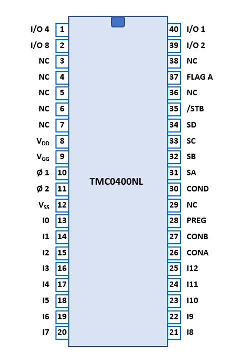
The TMC0400 uses a 0.6” wide 40-pin DIP (Dual In-line Package with a 0.1” / 2.54 mm lead pitch).
| Pin | IO | Function | Pin | IO | Function |
| 1 | IO | I/O Bus I/O 4 | 40 | IO | I/O Bus I/O 1 |
| 2 | IO | I/O Bus I/O 8 | 39 | IO | I/O Bus I/O 2 |
| 3 | n.c. | 38 | n.c. | ||
| 4 | n.c. | 37 | I | Flag A | |
| 5 | n.c. | 36 | Flag B | ||
| 6 | n.c. | 35 | I | Strobe | |
| 7 | n.c. | 34 | I | S-Times D | |
| 8 | V | VDD (0 V) | 33 | I | S-Times C |
| 9 | V | VGG (-7 V) | 32 | I | S-Times B |
| 10 | I | Clock In 1 | 31 | I | S-Times A |
| 11 | I | Clock In 2 | 30 | I | Condition Flag |
| 12 | V | VSS (+10 V) | 29 | n.c. | |
| 13 | O | ROM Instruction B0 | 28 | I | P Register |
| 14 | O | ROM Instruction B1 | 27 | I | Condition Flag B |
| 15 | O | ROM Instruction B2 | 26 | I | Condition Flag A |
| 16 | O | ROM Instruction B3 | 25 | O | ROM Instruction B12 |
| 17 | O | ROM Instruction B4 | 24 | O | ROM Instruction B11 |
| 18 | O | ROM Instruction B5 | 23 | O | ROM Instruction B10 |
| 19 | O | ROM Instruction B6 | 22 | O | ROM Instruction B9 |
| 20 | O | ROM Instruction B7 | 21 | O | ROM Instruction B8 |
If you have additions to the above datasheet please email: joerg@datamath.org.
© Joerg Woerner, March 7, 2021. No reprints
without written permission.