DATAMATH CALCULATOR MUSEUM
|
DATAMATH CALCULATOR MUSEUM |
Texas Instruments introduced on January 15, 1974 with the SR-50 their first "Slide Rule" calculator adding trigonometric and hyperbolic functions to the feature set of the SR-10, SR-11, and SR-16 line of calculators to compete with Hewlett Packard’s HP-35. The SR-50 was the first product based on the TMC0500 Building Blocks for Scientific and Programmable Calculators and used its minimum configuration combining the TMC0501 Arithmetic Chip and one TMC0521 SCOM (Scanning Read-Only Memory) Chip with the necessary display drivers for its 14-digit LED display, power supply and clock generation. Later Scientific Calculators made use of the flexibility of the TMC0500 architecture by using multiple SCOMs (SR-51), adding program and data memory (SR-56) and even magnetic card readers (SR-52) and a printer and matrix display (SR-60).
The Large Scale Integrated Circuits of the TMC0500 Building Blocks – like the TMS0200 Building Blocks for 12-digit Desktop and Printing calculators – were designed in a PMOS (P-channel Metal–oxide Semiconductor) process and require an external two-phase non-overlapping clock generator.
With the accuracy of the clock frequency for an electronic calculator not relevant, the first designs were based on a free-running multivibrator running during calculations at typically 250 kHz and applied to the PHI 1 and PHI 2 inputs of the PMOS chips. To lower the average power consumption of the calculator, during stand by operation (idle mode) the frequency is decreased to typically to around 80 kHz.
Requirements for the tolerance of the clock frequency applied to PHI 1 and PHI 2 inputs of the TMC0500 Building Blocks changed with the introduction of the SR-52 Programmable Calculator dramatically to ensure compatibility with one calculator writing magnetic cards and another device reading them. Texas Instruments had to control both motor speed of the four-track magnetic card read/write mechanism and data rate to and from the magnetic pick-up head very tightly due to the lack of any clocking pattern to synchronize the data at different rates.
The electronics of the SR-52 replaced the transistor-based, free-running multivibrator of the SR-50 with a more accurate design based on a mechanical resonator made of high-stability piezoelectric lead zirconate titanate (PZT). When connected to an electronic oscillator circuit, resonant mechanical vibrations in the device generate an oscillating signal of a specific frequency. Like the similar quartz crystal, they are used in oscillators for purposes such as generating the clock signal used to control timing in computers and other digital logic devices, or generating the carrier signal in analog radio transmitters and receivers.
The clock for the SR-52 PMOS chips is generated by the SN97211 Clock Generator Chip manufactured in bipolar technology with a ceramic resonator operating at a frequency of 384 kHz ± 1% and divided by two to produce a 192 kHz ± 1% two-phase clock with a 20% downtime. The TP0190N Clock Buffer Chip (actually a CD4011A Quad 2 Input NAND Gate specified for a supply voltage of 15.8 Volts) manufactured in CMOS technology conditions the signals to the proper levels of the TMC0500 Building Blocks.
The SN96239/SN97227 Clock Generator Chip was developed for the first version of the SR-50A/SR-51A and is variation of the SN97211. Instead of an accurate but expensive PZT together with three resistors and two capacitors, it is using a much simpler external circuitry with just two resistors and one capacitor to define its clock frequency.
The SN96239/SN97227 Clock Generator Chip was retired with the introduction of the SR-50A/SR-51A (Version 2) and SR-56 using the TMC0530 SCOM Chip with an integrated two-phase clock generator as a bond-out option.
SR-50A (Version 1), SR-51A (Version 1)
| Parameter | Min | Typ | Max | Unit | Comments |
| VSS | 0 | V | |||
| VBAT | -4.3 | -3.75 | -3.3 | V | |
| VGG | -16.3 | -15.8 | -15.3 | V | |
| IDD | 7.0 | mA | |||
| IDD | 1.0 | mA | |||
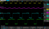
| PHI1, PHI2 | 125 165 |
kHz kHz |
/IDLE (VBAT) /IDLE (VSS) RA= 4.7 kOhm, RB= 5.1 kOhm C= 330 pF |
OSCILLATOR
The SN96239/SN97227 Clock Generator Chip uses an internal oscillator very similar to the NE555 circuitry with two external resistors and one external capacitor. The capacitor C is connected between OSC 1 and VBAT, a discharge resistor RB between OSC 1 and OSC 2 and a charge resistor RA between VSS and OSC 2. The output high-level duration tH and low-level duration tL can be calculated as follows:
tH = 0.8 (RA + RB) C
tL = 0.8 (RB) C
Recommended values for applications using the TMC0501 Arithmetic Chip are RA= 4.7 kOhm, RB= 5.1 kOhm and C= 330 pF resulting in tL = 2.6 µs and tH = 1.4 µs and a frequency of 250 kHz with /IDLE connected to VBAT. Connecting /IDLE to VSS increases the resulting frequency to about 330 kHz.FREQUENCY DIVIDER
The OSC 2 signal of the internal oscillator is divided with a negative-edge triggered Flip-Flop by two and the Q and /Q outputs of the Flip-Flop are masked with the OSC 2 signal to generate the two two-phase non-overlapping signals PHI 1 and PHI 2, respectively.
LEVEL SHIFTERS AND OUTPUT BUFFERS
The signal levels of the PHI 1 and PHI 2 signals are shifted with internal level shifters to voltages close to VSS and VGG but it is recommended to improve both their slew-rate and voltage swing with external buffers in CMOS technology like the CD4011 chip.
POWER SUPPLY CONSIDERATIONS
An external 10 µF filter capacitor across the VSS and VBAT pins is recommended to increase stability of the SN96239/SN97227 Clock Generator Chip and an extra diode connected in reverse between VBAT and VGG protects the device in case of VBAT discharging faster than VGG.
The SN96239/SN97227 was manufactured in a Bipolar process.
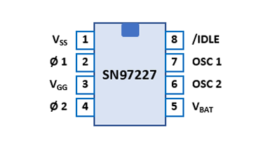
The SN96239/SN97227 uses a standard 0.3” wide 8-pin DIP (Dual In-line Package with a 0.1” / 2.54 mm lead pitch).
| Pin | IO | Function | Pin | IO | Function |
| 1 | V | Common Voltage | 8 | V | /IDLE (VBAT) |
| 2 | O | Clock Output 1 | 7 | A | OSC 1 (Threshold) |
| 3 | V | Negative Voltage VGG | 6 | O | OSC 2 (Discharge) |
| 4 | O | Clock Output 2 | 5 | V | Negative Voltage VBAT |
If you have additions to the above datasheet please email: joerg@datamath.org.
© Joerg Woerner, July 9, 2023. No reprints
without written permission.