DATAMATH CALCULATOR MUSEUM
|
DATAMATH CALCULATOR MUSEUM |
Texas Instruments introduced on January 15, 1974 with the SR-50 their first "Slide Rule" calculator adding trigonometric and hyperbolic functions to the feature set of the SR-10, SR-11, and SR-16 line of calculators to compete with Hewlett Packard’s HP-35. The SR-50 was the first product based on the TMS0500 Building Blocks for Scientific and Programmable Calculators and used its minimum configuration combining the TMC0501 Arithmetic Chip and one TMC0521 SCOM (Scanning Read-Only Memory) Chip with the necessary display drivers for its 14-digit LED display, power supply and clock generation. Later Scientific Calculators made use of the flexibility of the TMS0500 architecture by using multiple SCOMs (SR-51), adding program and data memory (SR-56) and even magnetic card readers (SR-52) and a printer and matrix display (SR-60).
The TMC0530 SCOM Chip integrates like its predecessor TMC0520 SCOM Chip 1,024*13 Bits Instruction Memory with serial interface to the TMC0501E Enhanced Arithmetic Chip, 16 Constants mainly used for the calculation of transcendental functions with 16 digits, each accessible through a 4-bit bidirectional I/O bus and outputs for up to 16-digit display and keyboard scanning. In addition to the 5 Registers of the TMC0501E Arithmetic Chip labeled A, B, C, D, and E integrates the SCOM Chip two additional Registers with 16 digits capacity each, and named accordingly Register F and Register G. Major improvement of the TMC0530 SCOM Chip is an additional integrated two-phase clock generator that can be used as a bond-out option in a 30-pin DIP (Dual Inline Package) encapsulation with an external mechanical resonator made of high-stability piezoelectric lead zirconate titanate (PZT) as used with the SR-52A or with reduced frequency stability in a standard 28-pin DIP housing as used with all other designs. While the design of the TMC0530 SCOM Chip would allow to use up to 8 devices in one product, were most designs implemented with additional TMC0560 BROM (Bare Read-Only Memory) Chips to increase program memory capacity.
Communication between the TMC0501E Enhanced Arithmetic Chip and the other family members of the TMS0500 Building Blocks is realized with multiple means:
|
• IDLE, PHI 1 and PHI 2
Signals are used to synchronize all peripherals connected to the TMC0501E
Enhanced Arithmetic Chip with the 16 States of its Instruction Cycle • EXT Output indicates that the TMC0501E Enhanced Arithmetic Chip is addressing external memories/registers • IRG Input to receive the 13-bit Instruction Words from the ROM of the TMC0530 • 4-bit bidirectional I/O Bus I/O 8, I/O 4, I/O 2, and I/O 1 to communicate with registers |
The TMC0530 SCOM Chip was replaced in Summer 1976 with the TMC0580 DSCOM (Double Scanning and Read-Only Memory) Chip boosting the program capacity from 1,024*13 Bits to 2.5k*13 Bits.
QUICK-LINK to TMS0500 Family.
| Type | Calculator | Function |
| TMC0531 | SR-50A (Version 2) | SCOM 1 |
| TMC0532 | SR-51A (Version 2) | SCOM 1 |
| TMC0533 | SR-51A (Version 2) | SCOM 2 |
| TMC0534 | SR-52A | SCOM 1, with TMC0562, TMC0563 |
| TMC0536 | SR-60 | SCOM 1, with TMC0564, TMC0565, TMC0566, TMC0567, TMC0568/TMC0570 |
| TMC0537 | SR-56 | SCOM 1 |
| TMC0538 | SR-56 | SCOM 2 |
| Revision | Products | First Prototypes | Comments |
| TMC0531 | SR-50A | (March 1975) | Initial design, SCOM 1 TMC0530 Base Mask rework |
| TMC0531 Rev A | SR-50A | December 1975 | |
| TMC0532 | SR-51A | May 1975 | Initial design, SCOM 1 Cos-1 hangup at -1 TMC0530 Base Mask rework |
| TMC0532 Rev A | SR-51A | November 1975 | |
| TMC0533 | SR-51A | May 1975 | Initial design, SCOM 2 Print Fix TMC0530 Base Mask rework |
| TMC0533 Rev A | SR-51A | November 1975 | |
| TMC0534 | SR-52A | December 1975 | Initial design, SCOM 1 ⅓ - ⅓ = 0 Fix |
| TMC0534 Rev A | SR-52A | [%] [=] [CE] 2 [SUM] 02 [RCL] 02 → -2 Stopped for TMC0534 Rev B |
|
| TMC0534 Rev B | SR-52A | August 1976 | |
| TMC0536 | SR-60 | ||
| TMC0537 | SR-51P (SR-56) | December 1975 | Initial design, SCOM 1 a ± 0b → a*1012 Fix ⅓ - ⅓ = 0 Fix, EE Goto |
| TMC0537 Rev A | SR-51P (SR-56) | March 1976 | [%] [=] [CE] 2 [SUM] 02 [RCL] 02 → -2 Stopped for TMC0534 Rev B (?) |
| TMC0538 | SR-51P (SR-56) | December 1975 | Initial design, SCOM 2 |
| SCOM | Top Markings Bottom Markings |
Calculator Date Code |
Instruction ROM ©Texas Instruments |
Constant ROM ©Texas Instruments |
Key Code Program ©Texas Instruments |
| TMC0531 Rev A | TMC0531NL AP7609 DP0531A SINGAPORE |
SR-50A LTA2676 |
|||
| TMC0532 Rev A | TMC0532NL KAΔ7606 K0532 JAPAN |
SR-51A LTA2976 |
|||
| TMC0533 Rev A | TMC0533NL AA7545 A 0533 |
NOS Q.C.S. |
|||
| TMC0533 Rev A | TMC0533NL AP7602 DP0533A SINGAPORE |
SR-51A LTA2976 |
|||
| TMC0534 Rev B | TMC0534NL BA7642 |
NOS Q.C.S. |
|||
| TMC0534 Rev B | TMC0534NL BSP7644 ● JP0534BS SINGAPORE |
SR-52A LTA0777 |
|||
| TMC0537 Rev A | TMC0537NL A7550 |
NOS Q.C.S. |
|||
| TMC0537 Rev A | TMC0537NL A7606 D 0537E |
SR-56 LTA0876 |
|||
| TMC0537 Rev A | TMC0537NL A7645 P0537I |
SR-56 RCI4976 |
|||
| TMC0538 Rev A | TMC0538NL A7606 D 0538 |
SR-56 LTA0876 |
|||
| TMC0538 Rev A | TMC0538NL A7644 P0538I |
SR-56 RCI4976 |
IMPORTANT NOTE: This information is provided as a service of the Datamath Calculator Museum to enthusiasts of early Texas Instruments calculators and please be aware that the Copyright of the Software transcribed in the ROM Images, the underlying algorithm or application might be owned by Texas Instruments or other third parties. The commercial use of the published Recorded ROM Images is strictly prohibited. In case of questions please contact us using the email address listed in the footer of this webpage.
| Item | Min | Typ | Max | Unit | Comments |
| VSS | 0 | V | |||
| VDD | -10.5 | -10.0 | -9.5 | V | |
| VGG | -16.3 | -15.8 | -15.3 | V | |
| PHI1, PHI2 | 192 | 195 | kHz | Opposite phases, 384 kHz PZT |
CLOCK GENERATOR
The main differentiator between the TMC0530 SCOM and its predecessor TMC0520 SCOM is the integrated two-phase clock generator. The TMS0500 Building Blocks use two non-overlapping clock signals with 180° phase difference and a voltage swing between VSS and VGG. While the original SR-50 design introduced in January 1974 featured a discrete circuitry for the clock generation consisting of a free-running multivibrator using two transistors and an additional four transistors to define both shape and voltage levels of the two clock signals, used the SR-50A introduced in March 1975 an integrated oscillator SN97227 and a TP4011 Clock Buffer Chip (actually a CD4011A Quad 2 Input NAND Gate specified for a supply voltage of 15.8 Volts) manufactured in CMOS technology to condition the signals to the proper levels of the TMS0500 Building Blocks.
The TMC0530 uses for the clock oscillator an additional bond pad on its die located between the VSS and D0 pins. Three different configurations are possible with the additional bond pad, depending on the target application:
|
• DIP-28 Encapsulation with
CLK signal bonded to Pin 14: Integrated clock oscillator, typical use
for SCOM 1 in SR-50A (Version 2), SCOM 2 SR-51A (Version 2) and SR-56 designs • DIP-28 Encapsulation with D0 signal bonded to Pin 14: Integrated clock oscillator disabled, typical use for SCOM 1 SR-51A (Version 2) and SR-56 designs to maintain PC-100 Printer Cradle compatibility • DIP-30 Encapsulation with CLK signal bonded to Pin 14 and D0 bonded to Pin 15: Integrated clock oscillator and D0 available for PC-100 Printer Cradle compatibility, typical use with SR-52A |
The integrated clock oscillator of the TMC0530 can be operated with three different circuitries to achieve the desired frequency stability:
|
• External resistor: Connecting
a resistor between the CLK pin and VGG
uses a small, internal capacitor of the TMC0530 to define the
frequency of the clock signal. A resistor value of 150 kOhm as used with the SR-50A (Version 2) and SR-51A (Version 2) results in a clock frequency around 150 - 180 kHz • External resistor and external capacitor: Connecting a resistor between the CLK pin and VGG and a capacitor to VSS results in an improved stability of the clock frequency. Values 30 kOhm and 39 pF as used with the SR-56 results in a clock frequency around 180 - 210 kHz • External resonator: Connecting a mechanical resonator made of high-stability piezoelectric lead zirconate titanate (PZT) between the CLK pin and VSS results in a very stability of the clock frequency allowing to write magnetic cards with one calculator and to read them with another one. The SR-52A uses a 384 kHz PZT resulting in a clock frequency of 192 kHz |
KEYBOARD AND DISPLAY SCANNING
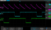
The TMS0500 Building Blocks use two non-overlapping clock signals PHI 1 and PHI 2 with a frequency of up to 250 kHz. Each so-called State Time consists of a sequence of PHI 1 → Pause 1 → PHI 2 → Pause 2 and represent the time for one bit to be operated on in the various sections of the chips. Sixteen of these State Times, numbered S0 to S15 represent one Digit Time used to scan the keyboard and display of the calculator. While the State Times count up from S0 → S1 ... → S15, are the Digit Times counting down from D15 → D14... → D0 to allow easier zero suppression approach of the displayed numbers. The TMC0501E Enhanced Arithmetic Chip generates an IDLE signal to synchronize the other TMC05XX chips to this timing sequence by marking the State Time S0 with its negative edge. The positive edge of the IDLE signal can occur anywhere between State Times S1 and S15, this feature is used to differentiate between the TMC0501E status "calculating" and "idle - display". Some calculator designs make use of the IDLE signal to lower the clock frequency in "display mode" to reduce power consumption of the chips.
The TMS0500 Building Blocks share both the tasks of scanning the keyboard and display with the SCOM/DSCOM Chips responsible to generate and output the 16 Digit Times Output in descending order on its D0 to D15 pins, while the Arithmetic Chip or Enhanced Arithmetic Chip reads the input of the keyboard matrix on its 7 KN to KT pins and outputs the decoded signals for the display on its 9 Segment Output pins SA to SH and DP.
INSTRUCTION MEMORY
The TMC0530 SCOM integrates a main Read-Only Memory (ROM) with 1,024*13 Bits as Instruction Memory for the TMC0501E Enhanced Arithmetic Chip. Internal, mask-programmed Chip-Select logic allow the use of a mix of up to 8 SCOM or TMC0560 BROM Chips in the design. With the Arithmetic Chip fetching the first instruction after power-on from Address 0, feature all known calculator designs based on the TMC0530 at least one SCOM addressed with the CS0 signal and hence covering an address range from 0x000 to 0x3FF (Decimal 0 to 1023). The innovative architecture of the TMS0500 Building Blocks allows not only the traditional loading of a ROM Address, additional logic inside the ROM addressing circuitry listens into the current instruction and based on additional signal even calculates the next ROM address. For this purpose the TMC0501E uses all 16 State Times S0 to S15 to communicate with its EXT Signal to the ROM Chips of the calculator:
|
• S0: PREG - Program
Register Signal to load the address counter with a 10-bit ROM Address • S1: COND - Condition Signal to allow for conditional branches • S2: HOLD - Hold Condition Signal to suppress auto-increment or decrement of the address counter • S3 - S12: lower 10-bit ROM Address (LSB first) • S13 - S15: upper 3-bit ROM Address (MSB last) for CS0 - CS7 |
The power-on circuitry of TMC0501E Enhanced Arithmetic Chip transmits on the EXT Signal for a few Digit Times a logical 1 at S0 time and logical 0 thereafter, effectively loading the address counter of the SCOM with 0x000 and selecting the ROM responding to CS0.
CONSTANT AND KEY CODE MEMORY
A novel feature of the TMS0500 Building Blocks is a dedicated space for constants, frequently used with computing algorithm of trigonometric functions like sine, cosine, or tangent and number conversions like millimeters to inches. With typical serial architectures used in electronic calculators, one instruction would load just one digit of a number and consequently for numbers represented in Scientific calculators with 12 to 15 digits, the algorithm would tend to be rather slow. Texas Instruments introduced with the TMS0500 Building Blocks a novel approach to load constants containing 16 digits within one Digit Time or instruction cycle from the Constant Memory to the TMC0501E Enhanced Arithmetic Chip. To overcome the limitations of a bit-serial data transfer, the TMS0500 Architecture includes a 4-bit bidirectional I/O Bus I/O 8, I/O 4, I/O 2, and I/O 1. One digit, each of the 16-digit constants is transmitted during access to the Constant Memory in one State Time. Addressing of one of the possible 128 16-digit constants is accomplished with the EXT Signal connected to the SCOM Chips and a Constant Select logic "listening" into the "Recall Constant" instruction on IRG and outputting the constants accordingly on the I/O Bus.
|
• S0: Always log.0 to Address Constant ROM • S3 - S5: Lower 3-bit Constant ROM Address (LSB first) • S7: Bit 4 of Constant ROM Address • S8 - S10: Upper 3-bit Constant ROM Address (MSB last) for CS0 - CS7 |
The TMC0530 SCOM stores up to 16 constants and all known Scientific calculators based on the TMS0500 Building Blocks use the same values in the Constant Memory:
| Constant Address |
16-digit SCOM Content (I/O 8 - 1, MSB first) |
Value c of Expression (≥ 13 digits) |
Expression |
| 00 | 230258509299400C | 2.302585092994 | c = ln (10) |
| 01 | 0693147180559945 | 0.69314718055995 | c = ln (2) |
| 02 | 0095310179804325 | 0.095310179804325 | c = ln (1.1) |
| 03 | 0009950330853168 | 0.0099503308531681 | c = ln (1.01) |
| 04 | 0000999500333084 | 0.00099950033308342 | c = ln (1.001) |
| 05 | 0000099995000333 | 0.000099995000333297 | c = ln (1.0001) |
| 06 | 0000009999950000 | 0.0000099999500003988 | c = ln (1.00001) |
| 07 | 0000000999999500 | 0.00000099999949991807 | c = ln (1.000001) |
| 08 | 0785398163397450 | 0.78539816339745 | c = arctan (1) |
| 09 | 0099668652491200 | 0.099668652491162 | c = arctan (0.1) |
| 0A | 0009999666686670 | 0.0099996666866652 | c = arctan (0.01) |
| 0B | 0000999999666667 | 0.00099999966666687 | c = arctan (0.001) |
| 0C | 0000099999999667 | 0.000099999999666667 | c = arctan (0.0001) |
| 0D | 157079632679501C | 1.57079632679486 | c = pi ÷ 2 |
| 0E | 314159265359000C | 3.141592653589793238 | c = pi |
| 0F | 572957795130801C | 5.729577951308 | c = 18 ÷ pi |
A second use of the Constant ROM in the TMC0530 SCOM was introduced with the SR-56, the TMC0538 stores Key Codes for its "Special Functions", an approach that was further developed in 1977 with the now legendary TI Programmable 59 for the Solid State Software Modules™ with up to 5,000 program steps in its TMC0540 PROM (Program Read-Only Memory).
SR-56 KEY CODES
The SR-56 Programmable Calculator can store a sequence of instructions in its TMC0599 Multi-Register Chip and execute them accordingly. The calculators provides with its [LRN] key the only way for the user to enter the instructions into the volatile Memory Chips but Texas Instruments introduced with the SR-56 a novel approach to store 128 mask-programmed Key Codes in the SCOM Chip:
|
• [LRN]: The instructions are
entered manually with keystrokes of the calculator keyboard into the Memory Chips • [CONST]: The instructions are copied from the Constant and Key Code SCOM into the Memory Chips |
The SR-56 Programmable Calculator uses the Decimal Numbers "00" to "99" for its Opcodes or Key Codes, most instructions are coded directly with their corresponding X/Y-position on the keyboard matrix with the keys [0]-[9] directly mapped into Key Codes 00 to 09:
| Key Code (BCD) |
_0 | _1 | _2 | _3 | _4 | _5 | _6 | _7 | _8 | _9 |
| 0_ | [0] | [1] | [2] | [3] | [4] | [5] | [6] | [7] | [8] | [9] |
| 1_ | [2nd][CLR] | [INV] | [lnx] | [eX] | [CLR] | [2nd][INV] | [2nd][log] | [2nd][10X] | ||
| 2_ | [2nd][1/x] | [GTO] | [sin] | [cos] | [tan] | [2nd][f(n)] (Note) |
[2nd][dsz] | [2nd][|x|] | [2nd][Int] | |
| 3_ | [2nd][PROD] | [x<>t] | [STO] | [RCL] | [SUM] | [2nd][x=t] | [2nd][CMs] | [2nd][EXC] | ||
| 4_ | [2nd][x√y] | [R/S] | [RST] | [x2] | [EE] | [yX] | [2nd][NOP] | [2nd][x≥t] | [2nd][√x] | [2nd][fix] |
| 5_ | [CE] | [(] | [)] | [÷] | [2nd][CP] | [2nd][subr] | [2nd][rtn] | [2nd][pause] | ||
| 6_ | [×] | [2nd][PI] | ||||||||
| 7_ | [−] | [2nd][RAD] | ||||||||
| 8_ | [+] | |||||||||
| 9_ | [.] | [+/−] | [=] | [2nd][prt] | [2nd][pap] | [2nd][listt] |
Note: Key Code "26" used for "Special Functions" has an
additional parameter: "00" [S.Dev.], "01" [Mean], "02" [[P→R], "03" [R→P], "04
[∑+] and "05" [∑−].
Please notice that the programs stored in the TMC0538 SCOM Chip have a combine lengths of 127 steps while [GTO] operations are limited to
a 2-digit addresses for a maximum of 99.
DATA REGISTERS
The TMC0530 provides two additional 16-digit Data Registers labeled Register F and Register G to the five Registers A - E of the TMC0501E Enhanced Arithmetic Chip. The Registers are implemented as Serial-Access Memories (SAMs) and use a similar mechanism for external access as the Constant ROM. The SCOM Chips "listen" into "Store F", "Store G", "Recall F", and "Recall G" instructions on IRG and communicate the 16-digit values over the 4-bit bidirectional I/O Bus I/O 8, I/O 4, I/O 2, and I/O 1. One digit, each of the 16-digit values is transmitted to or from the selected Data Register in one State Time between the TMC0501E and TMC0530 Chips. The SR-50A Scientific calculator uses the two external Data Registers to implement its Sum-of-Products Logic and providing one User Memory. The SR-51A, using two TMC0530 SCOM Chips is adding two additional User Memories to the calculator or allowing to run mean, variance, standard deviation and linear regression routines. The 9 available Registers of the SR-51 are used as follows:
| •
Register 1-4: Used for standard calculator operations • Register 5: Holding Register for second operand of multiplication or division and second operand of two-variable functions • Register 6: Sum-of-Products Register for intermediate results • Register 7-9: Memory Registers M1, M2 and M3 |
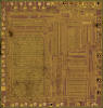
The TMC0530 was manufactured in a 8 um metal gate PMOS process (metal width = 0.3 mil / 8.0 um, metal spacing = 0.35 mil / 9.0 um, diffusion width = 0.25 mil / 6.0 um, diffusion spacing = 0.35 mil / 9.0 um).
The die size of the TMC0530 is approximately 185 mils * 195 mils / 4.7 mm * 5.0 mm.
The TMC0531, TMC0532, TMC0533, TMC0537, and TMC0538 use a standard 0.6” wide 28-pin DIP (Dual In-line Package with a 0.1” / 2.54 mm lead pitch).
The TMC0534 uses an unusual 0.6” wide 30-pin DIP (Dual In-line Package with a 0.1” / 2.54 mm lead pitch).
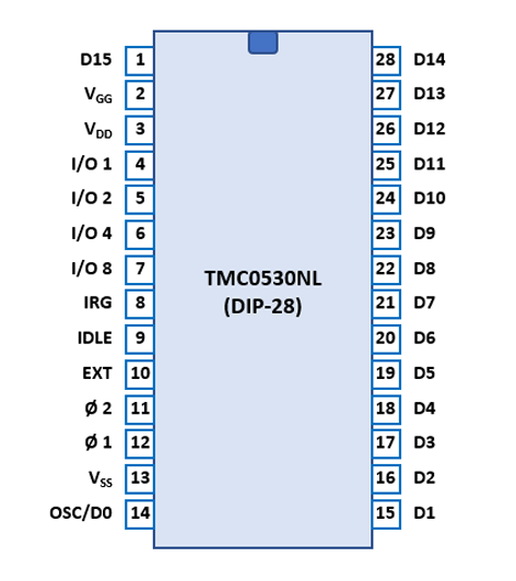 Pin Configuration 28-pin DIP
| Pin | IO | Function | Pin | IO | Function |
| 1 | O | Digit driver 14 | 28 | O | Digit driver 14 |
| 2 | V | Negative Voltage VGG | 27 | O | Digit driver 13 (OVER) |
| 3 | V | Negative Voltage VDD | 26 | O | Digit driver 12 (M-MSD) |
| 4 | IO | SCOM Interface D0 | 25 | O | Digit driver 11 |
| 5 | IO | SCOM Interface D1 | 24 | O | Digit driver 10 |
| 6 | IO | SCOM Interface D2 | 23 | O | Digit driver 9 |
| 7 | IO | SCOM Interface D3 | 22 | O | Digit driver 8 |
| 8 | O | Instruction words | 21 | O | Digit driver 7 |
| 9 | I | Calculating status | 20 | O | Digit driver 6 |
| 10 | I | External access | 19 | O | Digit driver 5 |
| 11 | IO | Clock Input/Output 2 | 18 | O | Digit driver 4 |
| 12 | IO | Clock Input/Output 1 | 17 | O | Digit driver 3 (M-LSD) |
| 13 | V | Common Voltage | 16 | O | Digit driver 2 (E-MSD) |
| 14 | XO | Oscillator/Digit driver 0 | 15 | O | Digit driver 1 (E-LSD) |
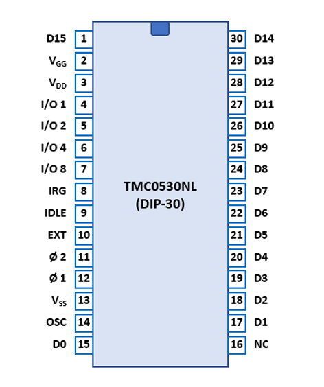 Pin Configuration
30-pin DIP
Pin Configuration
30-pin DIP| Pin | IO | Function | Pin | IO | Function |
| 1 | O | Digit driver 14 | 30 | O | Digit driver 14 |
| 2 | V | Negative Voltage VGG | 29 | O | Digit driver 13 (OVER) |
| 3 | V | Negative Voltage VDD | 28 | O | Digit driver 12 (E-MSD) |
| 4 | IO | SCOM Interface D0 | 27 | O | Digit driver 11 |
| 5 | IO | SCOM Interface D1 | 26 | O | Digit driver 10 |
| 6 | IO | SCOM Interface D2 | 25 | O | Digit driver 9 |
| 7 | IO | SCOM Interface D3 | 24 | O | Digit driver 8 |
| 8 | O | Instruction words | 23 | O | Digit driver 7 |
| 9 | I | Calculating status | 22 | O | Digit driver 6 |
| 10 | I | External access | 21 | O | Digit driver 5 |
| 11 | IO | Clock Input/Output 2 | 20 | O | Digit driver 4 |
| 12 | IO | Clock Input/Output 1 | 19 | O | Digit driver 3 (M-LSD) |
| 13 | V | Common Voltage | 18 | O | Digit driver 2 (E-MSD) |
| 14 | X | Oscillator | 17 | O | Digit driver 1 (E-LSD) |
| 15 | O | Digit driver 0 | 16 | - | Not connected |
The keyboards of all calculators based on the TMC0501E Arithmetic chip consist of an x/y-matrix connected to the SCOM digit driver outputs and the TMC0501E keymatrix inputs.
Example for the SR-50A with TMC0531:
| KN | KO | KP | KQ | KR | KS | KT | |
| D0 | |||||||
| D1 | 1 | = | C | log | eX | ∑ | |
| D2 | 2 | − | hyp | ||||
| D3 | 3 | + | . | x2 | D/R | ||
| D4 | 4 | arc | lnx | ||||
| D5 | 5 | ||||||
| D6 | 6 | ÷ | CE | 1/x | cos | STO | |
| D7 | 7 | × | +/− | sin | PI | ||
| D8 | 8 | RCL | |||||
| D9 | 9 | x<>y | |||||
| D10 | 0 | x√y | |||||
| D11 | xY | ||||||
| D12 | √x | ||||||
| D13 | EE | x! | tan | ||||
| D14 | [R-D] | ||||||
| D15 |
Notes: The R-D switch of the SR-50A is detected with a diode between D14 - KS.
Example for the SR-51A with TMC0532:
| KN | KO | KP | KQ | KR | KS | KT | |
| D0 | [PC100] | (1) | |||||
| D1 | 1 | = | C | eX | (1) | lnx | SUM |
| D2 | 2 | − | INV | (1) | |||
| D3 | 3 | + | . | x2 | (1) | PRM | |
| D4 | 4 | 2nd | (1) | % | |||
| D5 | 5 | (1) | |||||
| D6 | 6 | ÷ | CE | 1/x | (1) | cos | STO |
| D7 | 7 | × | +/− | (1) | sin | PI | |
| D8 | 8 | (1) | RCL | ||||
| D9 | 9 | (1) | ∑+ | ||||
| D10 | 0 | x√y | (1) | ||||
| D11 | xY | (1) | |||||
| D12 | (ADV) | (PRT) | √x | (1) | |||
| D13 | EE | x<>y | (1) | tan | |||
| D14 | (1) | [R-D] | |||||
| D15 | [TRC] | (1) |
Notes: The R-D switch is detected with a diode between D14 - KS. The PC-100 is detected with a diode between D0 - KP and the (PRT), (ADV) and [TRC] nodes are used to detect PRINT, PAPER ADVANCE and TRACE on the PC-100. The BUSY output of the TMC0251 Printer/Display Chip used with the PC-100 and PC-100A is connected to KR(1) and consequently active during all 16 Digit Times D0 to D15.
Example for the SR-52A with TMC0534:
| KN | KO | KP | KQ | KR | KS | KT | |
| D0 | [PC100] | (1) | |||||
| D1 | 1 | A | B | C | (1) | D | E |
| D2 | 2 | 2nd | INV | lnx | (1) | CE | CLR |
| D3 | 3 | LRN | sin | cos | (1) | tan | x√y |
| D4 | 4 | GTO | STO | RCL | (1) | SUM | YX |
| D5 | 5 | SBR | EE | ( | (1) | ) | ÷ |
| D6 | 6 | INS | (1) | × | |||
| D7 | 7 | SST | (1) | − | |||
| D8 | 8 | HLT | (1) | + | |||
| D9 | 9 | RUN | . | (1) | +/− | = | |
| D10 | 0 | [CS](1) | |||||
| D11 | (1) | ||||||
| D12 | (ADV) | (PRT) | (1) | ||||
| D13 | (1) | ||||||
| D14 | (1) | [R-D] | |||||
| D15 | [TRC] | (1) |
Notes: The R-D switch of the SR-52A is detected with a diode between D14 - KS and its Card Sense switch with a diode between D10 - KR. The PC-100 is detected with a diode between D0 - KP and the (PRT), (ADV) and [TRC] nodes are used to detect PRINT, PAPER ADVANCE and TRACE on the PC-100. The BUSY output of the TMC0251 Printer/Display Chip used with the PC-100 and PC-100A is connected to KR(1) and consequently active during all 16 Digit Times D0 to D15.
Example for the SR-56 with TMC0537:
| KN | KO | KP | KQ | KR | KS | KT | |
| D0 | [PC100] | (1) | |||||
| D1 | 1 | 2nd | INV | lnx | (1) | eX | CLR |
| D2 | 2 | LRN | GTO | sin | (1) | cos | tan |
| D3 | 3 | SST | x<>y | STO | (1) | RCL | SUM |
| D4 | 4 | R/S | RST | x2 | (1) | EE | YX |
| D5 | 5 | CE | ( | ) | (1) | ÷ | |
| D6 | 6 | (1) | × | ||||
| D7 | 7 | (1) | − | ||||
| D8 | 8 | (1) | + | ||||
| D9 | 9 | . | +/− | (1) | = | x<>y | |
| D10 | 0 | (1) | |||||
| D11 | (1) | ||||||
| D12 | (ADV) | (PRT) | (1) | ||||
| D13 | (1) | ||||||
| D14 | (1) | [R-D] | |||||
| D15 | [TRC] | (1) |
Notes: The R-D switch of the SR-56 is detected with a diode between D14 - KS. The PC-100 is detected with a diode between D0 - KP and the (PRT), (ADV) and [TRC] nodes are used to detect PRINT, PAPER ADVANCE and TRACE on the Printer Cradle PC-100. The BUSY output of the TMC0251 Printer/Display Chip used with the PC-100 and PC-100A is connected to KR(1) and consequently active during all 16 Digit Times D0 to D15.
If you have additions to the above datasheet please email: joerg@datamath.org.
© Joerg Woerner, December 28, 2020. No reprints
without written permission.