DATAMATH CALCULATOR MUSEUM
|
DATAMATH CALCULATOR MUSEUM |
Texas Instruments introduced in January 1974 with the SR-50 a product utilizing only the bare minimum of the capabilities of the TMS0500 Building Blocks for Scientific and Programmable Calculators but the subsequent introduction of the SR-52 Programmable and the PC-100 Printer Cradle clearly demonstrated the scalability of this groundbreaking architecture. While the SR-52 included an internal reader for magnetic cards to store and load programs with up to 224 steps, lacked the lower-end SR-56 any means to archive its programs and the user had to enter the program manually after turning the power switch into the On position. With just 100 program steps available for the user of the SR-56, an annoying but acceptable approach. Things changed dramatically when Texas Instruments introduced in May 1977 with the TI-58 its successor offering a maximum of 480 program steps and the calculator had still no external or internal media to archive them. Texas Instruments consequently introduced in March 1979 the TI-58C with Continuous Memory, meaning that both user program and user data are maintained even if the power off condition. Instead of porting the TMC0598 Multi-Register Chips designed in power-hungry PMOS technology used with the TI-58 into modern CMOS technology, the engineering team decided to use a standard SRAM (Static Random Access Memory) manufactured in a power-saving CMOS process and developed with the TMC0590 Continuous Memory Interface Chip a TMS0500 Building Block to translate the signals of the TMC0501E Arithmetic Chip to the common signals of SRAMs with a capacity of 1k*4 Bits.
The TMC0501E Arithmetic Chip uses a total of nine signals to communicate in the TI-58 with the TMC0598 Multi-Register Chips:
|
• IDLE, PHI 1 and PHI 2
Signals are used to synchronize all peripherals connected to the TMC0501E Arithmetic Chip with the 16 States of its Instruction Cycle • EXT Output indicates that the TMC0501E Arithmetic Chip is addressing external memories/registers • IRG Input to receive the 13-bit Instruction Words from the TMC0520/TMC0530/TMC0540/TMC0560/TMC0580 ROM Chips • 4-bit bidirectional I/O Bus I/O 8, I/O 4, I/O 2, and I/O 1 to communicate with Multi-Register Chips and other peripherals |
Standard SRAMs use a completely different approach to interface with Microprocessors and use the following signals:
|
• Bidirectional Data Signals Data I/On-1 – Data I/O0 with n being the width of the Data Bus • Address Signals Am-1 – A0 to address up to 2m Data Words • /CE Chip Enable Input to activate the SRAM and switch from low-power data retention mode to active mode • /WE Write Enable to store the Data Word applied to Dn-1 – D0 into the memory cells addressed with the signals Am-1 – A0 • /OE Output Enable to control the direction of the bidirectional Data Signals |
With the TMC0598 Multi-Register Chips manufactured in PMOS technology and powered with VDD = -10V and CMOS SRAMs powered with VDD = +5V, the TMC0590 Continuous Memory Interface Chip performs three main functions:
|
• Converting the TMS0500 communication protocol to the standard SRAM interface • Translating the PMOS levels of the TMC0501E Arithmetic Chip to the CMOS levels of the SRAM • Enabling and disabling the low-power data retention mode of the CMOS SRAM |
Texas Instruments used with the first design of the TI-58C a 1k*4 Bits CMOS SRAM manufactured by RCA, the inventor of CMOS technology, with a TI internal part number in a 18-pin DIP (Dual In-line Plastic) encapsulation. We assume the part is actually a MW5114 chip sporting only /CE and /WE signals while the second design of the TI-58C makes use of either a Toshiba TC5047AP or NEC uPD445L chip in a 20-pin DIP housing and featuring in addition to the /CE, /WE, and /OE signals an unused CE2 pin.
The TI-58C uses an additional -5 Volt power supply fed to the GND pin of the CMOS SRAM while its VDD pin is tied to the VSS pin of the PMOS devices. When the calculator is turned off, a Germanium diode with a low voltage drop connects the GND pin of the CMOS RAM to the negative battery terminal to provide the voltage necessary for data retention in this state. An additional 470 µF capacitor connected in parallel to the battery keeps the memory safe for a few minutes even in case the battery pack is replaced.
| Node | Voltage | PMOS | CMOS | Comments |
| Battery + | 0 V | VSS | VDD | |
| Battery - | -3.75 V | GND | Retention Mode | |
| VDD2 | -5.0 V | GND | Active Mode | |
| VDD | -10.0 V | VDD | ||
| VGG | -15.8 V | VGG |
The only known application of the TMC0590 Continuous Memory Interface Chip is the TMC0591 chip used with both the first and second design of the TI-58C.
QUICK-LINK to TMS0500 Family.
| Type | Calculators | Function |
| TMC0591 | TI-58C (1979), TI-58C (1980) | Continuous Memory Interface |
| Item | Min | Typ | Max | Unit | Comments |
| VSS | 0 | V | |||
| VDD2 | -4.3 | -3.75 | -3.3 | V | Retention Mode |
| VDD2 | -5.5 | -5.0 | -4.5 | V | Active Mode |
| VDD | -10.5 | -10.0 | -9.5 | V | |
| PHI1, PHI2 | 225 | 230 | kHz | Opposite phases |
The TMC0590 was manufactured in a 6 um metal gate PMOS process (metal width = 0.25 mil / 6.0 um, metal spacing = 0.30 mil / 8.0 um, diffusion width = 0.25 mil / 6.0 um, diffusion spacing = 0.30 mil / 8.0 um).
The die size of the TMC0590 is approximately 145 mils * 120 mils / 3.7 mm * 3.0 mm.
The TMC0590 uses a 0.4” wide 28-pin SPDIP (Shrink Plastic Dual In-line Package with a 0.07” / 1.778 mm lead pitch).
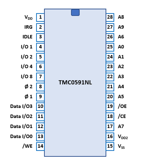
| Pin | IO | Function | Pin | IO | Function |
| 1 | V | Negative Voltage VDD | 28 | O | SRAM Address A8 |
| 2 | I | Instruction words | 27 | O | SRAM Address A9 |
| 3 | I | Calculating status | 26 | O | SRAM Address A6 |
| 4 | IO | ARITH Interface D0 | 25 | O | SRAM Address A0 |
| 5 | IO | ARITH Interface D1 | 24 | O | SRAM Address A1 |
| 6 | IO | ARITH Interface D2 | 23 | O | SRAM Address A2 |
| 7 | IO | ARITH Interface D3 | 22 | O | SRAM Address A3 |
| 8 | I | Clock Input 2 | 21 | O | SRAM Address A4 |
| 9 | I | Clock Input 1 | 20 | O | SRAM Address A5 |
| 10 | IO | SRAM Data I/O3 | 19 | O | SRAM Output Enable |
| 11 | IO | SRAM Data I/O2 | 18 | O | SRAM Chip Enable |
| 12 | IO | SRAM Data I/O1 | 17 | O | SRAM Address A7 |
| 13 | IO | SRAM Data I/O0 | 16 | V | Negative Voltage VDD2 |
| 14 | O | SRAM Write Enable | 15 | V | Common Voltage |
If you have additions to the above datasheet please email: joerg@datamath.org.
© Joerg Woerner, March 02, 2021. No reprints
without written permission.