DATAMATH CALCULATOR MUSEUM
|
DATAMATH CALCULATOR MUSEUM |
Texas Instruments introduced on January 15, 1974 with the SR-50 their first "Slide Rule" calculator adding trigonometric and hyperbolic functions to the feature set of the SR-10, SR-11, and SR-16 line of calculators to compete with Hewlett Packard’s HP-35. The SR-50 was the first product based on the TMS0500 Building Blocks for Scientific and Programmable Calculators and used its minimum configuration combining the TMC0501 Arithmetic Chip and one TMC0521 SCOM (Scanning Read-Only Memory) Chip with the necessary display drivers for its 14-digit LED display, power supply and clock generation. Later Scientific Calculators made use of the flexibility of the TMC0500 architecture by using multiple SCOMs (SR-51), adding program and data memory (SR-56) and even magnetic card readers (SR-52) and a printer and matrix display (SR-60).
The TMC0599 Multi-Register Chip integrates 240*8 Bits RAM (Random Access Memory) storing 240 program steps or 30 numbers of 16 digits, each and accessible through a 4-bit bidirectional I/O bus. The design of the TMC0599 with one Chip Select (C.S.) and two Address pins (ADD0, ADD 1) allows for both compact designs with stacking two by two chips, each in a piggyback manner with cutting one of the two Address pins and large designs with an external address decoder activating the Chip Select pin:
| Address | TMC0599 Stack 1 | TMC0599 Stack 2 | ||
| Chip Position | Top Chip | Bottom Chip | Top Chip | Bottom Chip |
| ADD 0 | n.c. | VSS | n.c. | VSS |
| ADD 1 | n.c. | n.c. | VSS | VSS |
| C.S. | n.c. | n.c. | n.c. | n.c. |
| Active Bank | Bank 0 | Bank 1 | Bank 2 | Bank 3 |
Communication between the TMC0501 Arithmetic Chip to the TMC0599 Multi-Register Chip is realized with multiple means:
|
• IDLE, PHI 1 and PHI 2
Signals are used to synchronize all peripherals connected to the TMC0501 Arithmetic Chip with the 16 States of its Instruction Cycle • EXT Output indicates that the TMC0501 Arithmetic Chip is addressing external memories/registers • IRG Input to receive the 13-bit Instruction Words from the ROM of the TMC0520/TMC0530/TMC0560 • 4-bit bidirectional I/O Bus I/O 8, I/O 4, I/O 2, and I/O 1 to communicate with registers |
The TMC0599 Multi-Register Chip was replaced in 1977 with the TMC0598 dropping the negative VGG supply voltage.
QUICK-LINK to TMS0500 Family.
| Calculator | Program steps | Data memory | TMC0599 |
| SR-52 | 224 | 20 | 2 |
| SR-56 | 100 | 10 | 1 |
| SR-60 | 480 | 40 | 5 |
| SR-60A | 1920 | 100 | 13 |
| Revision | Products | First Prototypes | Comments |
| TMC0599 | SR-52, SR-60 | Initial design (indecipherable) |
|
| TMC0599 Rev A | SR-52, SR-60 | Loosing Bits | |
| TMC0599 Rev B | SR-52, SR-60 | April 1975 | Frequency |
| TMC0599 Rev C | SR-52, SR-60 | Bad Voltage | |
| TMC0599 Rev D | SR-52, SR-60 | ||
| TMC0599 Rev D | SR-52, SR-60 | ||
| TMC0599 Rev E | SR-52 II (TI-59) | November 1976 | Single Voltage Renamed to TMC0598 |
| Item | Min | Typ | Max | Unit | Comments |
| VSS | 0 | V | |||
| VDD | -10.5 | -10.0 | -9.5 | V | |
| VGG | -16.3 | -15.8 | -15.3 | V | |
| PHI1, PHI2 | 225 | 230 | kHz | Opposite phases |
The TMC0599 was manufactured in a 8 um metal gate PMOS process (metal width = 0.30 mil / 8.0 um, metal spacing = 0.30 mil / 8.0 um, diffusion width = 0.25 mil / 6.0 um, diffusion spacing = 0.35 mil / 9.0 um).
The die size of the TMC0598 is approximately 210 mils * 140 mils / 5.3 mm * 3.6 mm.
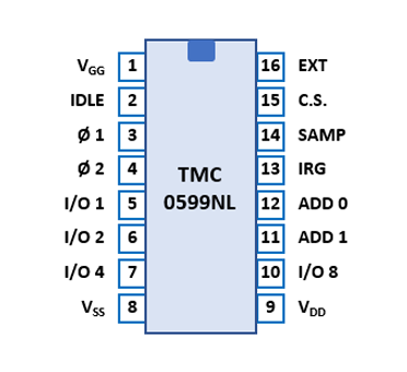
The TMC0599 uses a standard 0.3” wide 16-pin DIP (Dual In-line Package with a 0.1” / 2.54 mm lead pitch).
| Pin | IO | Function | Pin | IO | Function |
| 1 | V | Negative Voltage VGG | 16 | I | External access |
| 2 | I | Calculating status | 15 | I | CS (not connected) |
| 3 | I | Clock Input 1 | 14 | I | SAMP (not connected) |
| 4 | I | Clock Input 2 | 13 | O | Instruction words |
| 5 | IO | SCOM Interface D0 | 12 | I | Bank-Select 1 (VSS, nc) |
| 6 | IO | SCOM Interface D1 | 11 | I | Bank-Select 0 (VSS, nc) |
| 7 | IO | SCOM Interface D2 | 10 | IO | SCOM Interface D3 |
| 8 | V | Common Voltage | 9 | V | Negative Voltage VDD |
If you have additions to the above datasheet please email: joerg@datamath.org.
© Joerg Woerner, February 02, 2001. No reprints
without written permission.