DATAMATH CALCULATOR MUSEUM
|
|
DATAMATH CALCULATOR MUSEUM |
Characterization of Single-chip Calculator Circuits - TMS1070 Family
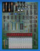
The DCM-50A Platform supports the Characterization of TMS1070 Devices in its rightmost TMS1000 Textool Test Socket with patching of Pin 20 and Pin 21 and the voltages VSS set to 9.5V and VDD/VGG set to -5.5V, accordingly with the MOS-Load resistors tied to VDD, simulating the low-voltage Vacuum Fluorescent Displays (VFDs) used with all TMS1070 calculator designs.
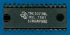
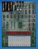
![]() Device-under-Test:
Device-under-Test:
| • Package Markings Top: TMS1071NL, AP 7545 • Package Markings Bottom: JP1071, SINGAPORE • Donor Calculator: TI-2550 II, LTA 0976 |
Keyboard: The TI-2550 II makes use of a keyboard with snap-action
dome switches arranged in a 7*4 matrix with the rows connected to the R0-R6 Outputs (Display Scan) and the columns connected to the K1-K8 Inputs (Keyboard Scan) of the TMS1071NL
single-chip calculator circuit. The [F - 2] sliding switch is connected between the R9
Output and K2 Input.
While the TI-2550 II doesn't show a physical [+/-]
key, is its snap action switch on the keyboard actually fully functional. The [F
- 2] switch selects between displaying results with a floating decimal and up to
seven digits to the right of the decimal point or rounding the results to two
decimal places. Connecting the R9 Output to the K1 or K4 Inputs results in one
or four decimal places, accordingly. Connecting the R9 Output to the K8 Input
yields to expected erratic behavior.
Keyboard Matrix of the TI-2550 II:
| K1 | K2 | K4 | K8 | |
| R0 (D1) | CE | 0 | . | = |
| R1 (D2) | 1 | 2 | 3 | + |
| R2 (D3) | 4 | 5 | 6 | − |
| R3 (D4) | 7 | 8 | 9 | × |
| R4 (D5) | RV | C | % | ÷ |
| R5 (D6) | CM | MR | M− | M+ |
| R6 (D7) | (+/−) | √x | x2 | 1/x |
| R7 (D8) | ||||
| R8 (D9) | ||||
| R9 | ([F - 1]) | [F - 2] | ([F - 4]) | |
| R10 |
Notes: (x) Implemented in TMS1071NL but not available on TI-2550 II. [y z] Sliding Switch Function, y Switch open, z Switch closed
![]() Display: The TI-2550 II makes use of a 9-digit Itron
FG95A1 low-voltage Vacuum Fluorescent Display (VFD) connected directly to the
respective 9 R Outputs (Display Scan) and 8 O Outputs (Segments) of the
TMS1071NL and biased to approximately -25 Volts with discrete pull-down
resistors.
Display: The TI-2550 II makes use of a 9-digit Itron
FG95A1 low-voltage Vacuum Fluorescent Display (VFD) connected directly to the
respective 9 R Outputs (Display Scan) and 8 O Outputs (Segments) of the
TMS1071NL and biased to approximately -25 Volts with discrete pull-down
resistors.
Display Layout:
| Itron FG95A1 |
|
|
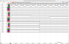
The Output Decoder PLA of the TMS1071NL is programmed for 7-Segment displays with the following Output Assignments:
| TMS1071 Pin | 17 | 16 | 15 | 14 | 13 | 12 | 11 | 10 |
| TMS1071 Port | O0 | O1 | O2 | O3 | O4 | O5 | O6 | O7 |
| Segment | A | B | C | D | E | F | G | DP |
| The Segment drivers A-G and DP (Decimal Point) are connected to the Itron FG95A1 display in the pictured way. | 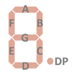 |
Display Fonts:
| Type | Calculator | Number Fonts | Decimal Separator |
Thousands Separator |
Entry Overflow |
Calculating Overflow |
Minus | Memory Indicator |
| TMS1071NL | TI-2550 II | n.a. |
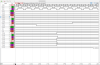
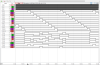
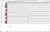
 Scanning: Display and keyboard scanning is performed in R8 → R0 direction at a rate of about 260 Hz
with one Blank State after R0:
Scanning: Display and keyboard scanning is performed in R8 → R0 direction at a rate of about 260 Hz
with one Blank State after R0:
|
• Instruction Cycle Time
(ICT) = 6 Clocks = 0.02 ms @ CK=300 kHz • Leading Digit Blanking Time = 2 ICT = 0.04 ms • Active Digit Time = 16 ICT = 0.32 ms • Trailing Digit Blanking = 2 ICT = 0.04 ms • Blank State R0 → R8 = 13 ICT = 0.26 ms • Display Cycle Time = 193 ICT = 3.86 ms |
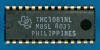
![]() Device-under-Test:
Device-under-Test:
| • Package Markings Top: TMC1073NL,
DS 8131, PHILIPPINES • Package Markings Bottom: NONE • Donor Calculator: TI-5100, ATA 5081 |
Keyboard: The TI-5100 makes use of a keyboard with
spring-loaded switches arranged in a 6*4 matrix with the rows connected to the R5-R10 Outputs (Display Scan) and the columns connected to the K1-K8 Inputs (Keyboard Scan) of the TMC1073NL
single-chip calculator circuit. The [K - C] and [F - 2] sliding switches are connected between the
R0 and R2
Outputs and K8 Input.
The TI-5100 doesn't use all features
programmed into the TMC1073NL chip, don't miss the Toshiba BC-1015 unleashing some
additional functionality.
Keyboard Matrix of the TI-5100:
| K1 | K2 | K4 | K8 | |
| R0 (D1) | [K - C] | |||
| R1 (D2) | ||||
| R2 (D3) | [F - 2] | |||
| R3 (D4) | ||||
| R4 (D5) | (EX) | (GPM) | (Δ%) | |
| R5 (D6) | C/CE | CM | N | % |
| R6 (D7) | 0 | 1 | 4 | 7 |
| R7 (D8) | 2 | 5 | 8 | |
| R8 (D9) | . | 3 | 6 | 9 |
| R9 (D10) | += | −= | × | |
| R10 (D11) | M+= | M−= | RM | ÷ |
Notes: (x) Implemented in TMC1073NL but not available on TI-5100. [y z] Sliding Switch Function, y Switch open, z Switch closed
![]() Display: The TI-5100 makes use of an
11-digit Itron
FG119A1 low-voltage Vacuum Fluorescent Display (VFD) connected directly to the
respective 11 R Outputs (Display Scan) and 8 O Outputs (Segments) of the
TMC1073NL and biased to approximately -32 Volts with discrete pull-down
resistors. While the original TMS0100
single-chip calculator circuit included 9 Segment Outputs for 7-Segment displays
with either an additional segment available for "fancy fours" or a comma to group
thousands, dropped the TMS1000 and this
related TMS1070 the 9th Segment Output and Texas Instruments
consequently introduced a novel approach to drive the extra segment of the
FG119A1 display. Output R10, one of the 11 R Outputs used for Display and
Keyboard Scan, is not only connected to the left-most digit of the display but
the comma indicator, too and activated together with the desired digits. Please
notice the additional patch wire connecting Pin 13 (Digit driver 11) and Pin 23
(Segment driver H) at the TMS0100 socket to simulate this behavior with the
DCM-50A Platform.
Display: The TI-5100 makes use of an
11-digit Itron
FG119A1 low-voltage Vacuum Fluorescent Display (VFD) connected directly to the
respective 11 R Outputs (Display Scan) and 8 O Outputs (Segments) of the
TMC1073NL and biased to approximately -32 Volts with discrete pull-down
resistors. While the original TMS0100
single-chip calculator circuit included 9 Segment Outputs for 7-Segment displays
with either an additional segment available for "fancy fours" or a comma to group
thousands, dropped the TMS1000 and this
related TMS1070 the 9th Segment Output and Texas Instruments
consequently introduced a novel approach to drive the extra segment of the
FG119A1 display. Output R10, one of the 11 R Outputs used for Display and
Keyboard Scan, is not only connected to the left-most digit of the display but
the comma indicator, too and activated together with the desired digits. Please
notice the additional patch wire connecting Pin 13 (Digit driver 11) and Pin 23
(Segment driver H) at the TMS0100 socket to simulate this behavior with the
DCM-50A Platform.
Display Layout:
| Itron FG119A1 |
|
|
The Output Decoder PLA of the TMC1073NL is programmed for 7-Segment displays with the following Output Assignments:
| TMC1073 Pin | 17 | 16 | 15 | 14 | 13 | 12 | 11 | 10 |
| TMC1073 Port | O0 | O1 | O2 | O3 | O4 | O5 | O6 | O7 |
| Segment | A | B | C | D | E | F | G | DP |
| The Segment drivers A-G, DP (Decimal Point) and CP (Comma) are connected to the Itron FG119A1 display in the pictured way. | 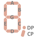 |
Display Fonts:
| Type | Calculator | Number Fonts | Decimal Separator |
Thousands Separator |
Entry Overflow |
Calculating Overflow |
Minus | Memory Indicator |
| TMC1073NL | TI-5100 |
The Memory, Minus, and Overflow Indicators of the Itron FG119A1 display are connected to Segments B, G, and A of the numbers, respectively.
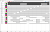
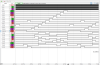
 Scanning: Display and keyboard scanning is performed in R0 → R10 direction at a rate of about
120-150 Hz with one Blank State after R10. Active Digit Time is stretched when
displaying up to three Comma Indicators (Thousands):
Scanning: Display and keyboard scanning is performed in R0 → R10 direction at a rate of about
120-150 Hz with one Blank State after R10. Active Digit Time is stretched when
displaying up to three Comma Indicators (Thousands):
|
• Instruction Cycle Time
(ICT) = 6 Clocks = 0.02 ms @ CK=300 kHz • Leading Digit Blanking Time = 1 ICT = 0.02 ms • Active Digit Time = 26 ICT = 0.52 ms • Active Digit Time (Stretched) = 57 ICT = 1.14 ms • Trailing Digit Blanking = 1 ICT = 0.02 ms • Blank State R10 → R0 = 26 ICT = 0.52 ms • Display Cycle Time = 334-427 ICT = 6.68-8.54 ms |

 Device-under-Test:
| • Package Markings Top: TMC1073NL,
MSL 7901, SINGAPORE • Package Markings Bottom: NONE • Donor Calculator: Toshiba BC-1015, April 1979 |
Keyboard: The Toshiba BC-1015 makes use of a keyboard with conductive rubber switches arranged in a 7*4 matrix with the rows connected to the R4-R10 Outputs (Display Scan) and the columns connected to the K1-K8 Inputs (Keyboard Scan) of the TMC1073NL single-chip calculator circuit. The [ - K] and [F - 2] sliding switches are connected between the R0 and R2 Outputs and K8 Input.
Keyboard Matrix of the Toshiba BC-1015:
| K1 | K2 | K4 | K8 | |
| R0 (D1) | [ - K] | |||
| R1 (D2) | ||||
| R2 (D3) | [F - 2] | |||
| R3 (D4) | ||||
| R4 (D5) | EX | GPM | Δ% | |
| R5 (D6) | C/CE | CM | IC | % |
| R6 (D7) | 0 | 1 | 4 | 7 |
| R7 (D8) | 2 | 5 | 8 | |
| R8 (D9) | . | 3 | 6 | 9 |
| R9 (D10) | += | −= | × | |
| R10 (D11) | M+= | M−= | RM | ÷ |
Notes: [y z] Sliding Switch Function, y Switch open, z Switch closed
![]() Display: The
Toshiba BC-1015 makes use of an
11-digit Futaba 11-BT-16A low-voltage Vacuum Fluorescent Display (VFD) connected directly to the
respective 11 R Outputs (Display Scan) and 8 O Outputs (Segments) of the
TMC1073NL and biased to approximately -30 Volts with discrete pull-down
resistors. While the original TMS0100
single-chip calculator circuit included 9 Segment Outputs for 7-Segment displays
with either an additional segment available for "fancy fours" or a comma to group
thousands, dropped the TMS1000 and this
related TMS1070 the 9th Segment Output and Texas Instruments
consequently introduced a novel approach to drive the extra segment of the
11-BT-16A display. Output R10, one of the 11 R Outputs used for Display and
Keyboard Scan, is not only connected to the left-most digit of the display but
the comma indicator, too and activated together with the desired digits. Please
notice the additional patch wire connecting Pin 13 (Digit driver 11) and Pin 23
(Segment driver H) at the TMS0100 socket to simulate this behavior with the
DCM-50A Platform.
Display: The
Toshiba BC-1015 makes use of an
11-digit Futaba 11-BT-16A low-voltage Vacuum Fluorescent Display (VFD) connected directly to the
respective 11 R Outputs (Display Scan) and 8 O Outputs (Segments) of the
TMC1073NL and biased to approximately -30 Volts with discrete pull-down
resistors. While the original TMS0100
single-chip calculator circuit included 9 Segment Outputs for 7-Segment displays
with either an additional segment available for "fancy fours" or a comma to group
thousands, dropped the TMS1000 and this
related TMS1070 the 9th Segment Output and Texas Instruments
consequently introduced a novel approach to drive the extra segment of the
11-BT-16A display. Output R10, one of the 11 R Outputs used for Display and
Keyboard Scan, is not only connected to the left-most digit of the display but
the comma indicator, too and activated together with the desired digits. Please
notice the additional patch wire connecting Pin 13 (Digit driver 11) and Pin 23
(Segment driver H) at the TMS0100 socket to simulate this behavior with the
DCM-50A Platform.
Display Layout:
| Futaba 11-BT-16A |
|
|
The Output Decoder PLA of the TMC1073NL is programmed for 7-Segment displays with the following Output Assignments:
| TMC1073 Pin | 17 | 16 | 15 | 14 | 13 | 12 | 11 | 10 |
| TMC1073 Port | O0 | O1 | O2 | O3 | O4 | O5 | O6 | O7 |
| Segment | A | B | C | D | E | F | G | DP |
| The Segment drivers A-G, DP (Decimal Point) and CP (Comma) are connected to the Futaba 11-BT-16A display in the pictured way. | 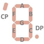 |
Display Fonts:
| Type | Calculator | Number Fonts | Decimal Separator |
Thousands Separator |
Entry Overflow |
Calculating Overflow |
Minus | Memory Indicator |
| TMC1073NL | BC-1015 |
The Overflow, Minus, and Memory Indicators of the Futaba 11-BT-16A display is connected to Segments A, G, and B of the numbers, respectively.
Scanning: Display and keyboard scanning is performed in R0 → R10 direction at a rate of about
120-150 Hz with one Blank State after R10. Active Digit Time is stretched when
displaying up to three Comma Indicators (Thousands):
|
• Instruction Cycle Time
(ICT) = 6 Clocks = 0.02 ms @ CK=300 kHz • Leading Digit Blanking Time = 1 ICT = 0.02 ms • Active Digit Time = 26 ICT = 0.52 ms • Active Digit Time (Stretched) = 57 ICT = 1.14 ms • Trailing Digit Blanking = 1 ICT = 0.02 ms • Blank State R10 → R0 = 26 ICT = 0.52 ms • Display Cycle Time = 334-427 ICT = 6.68-8.54 ms |
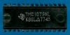 Device-under-Test:
| • Package Markings Top: TMC1079NL,
KBSLΔ7745 • Package Markings Bottom: NONE • Donor Calculator: Canon Palmtronic MD-8, December 1977 |
Keyboard: The Canon Palmtronic MD-8 makes use of a keyboard with conductive rubber switches arranged in a 10*3 matrix with the rows connected to the R0-R9 Outputs (Display Scan) and the columns connected to the K2-K8 Inputs (Keyboard Scan) of the TMC1079NL single-chip calculator circuit. The [MEMORY - SINGLE - PROCESS] and [ - AM] sliding switches are connected between the R10 Output and K1 and K2 Inputs.
Keyboard Matrix of the Canon Palmtronic MD-8:
| K1 | K2 | K4 | K8 | |
| R0 (D1) | %± | . | 0 | |
| R1 (D2) | = | RM | 1 | |
| R2 (D3) | ÷ | SC | 2 | |
| R3 (D4) | × | CM | 3 | |
| R4 (D5) | + | √x | 4 | |
| R5 (D6) | − | M+ | 5 | |
| R6 (D7) | RV | 6 | ||
| R7 (D8) | 7 | |||
| R8 (D9) | (C) | 8 | ||
| R9 (D10) | CI/C | 9 | ||
| R10 (D11) | [M-S-P] | [ - AM |
Notes: (x) Implemented in TMC1079NL but not available on Canon Palmtronic MD-8. [y z] Sliding Switch Function, y Switch open, z Switch closed
![]() Display: The
Canon Palmtronic MD-8 makes use of a two-line 9-digit Futaba 20-ST-22 low-voltage Vacuum Fluorescent Display (VFD)
with one additional Grid-Pair for the Memory and Basic Function Indicator. A
novel layout of the 20-digit VFD allows the TMC1079NL to fully control it with
the available 11 R Outputs (Display Scan) and 8 O Outputs (Segments): All Anodes
of the VFD are connected in the usual way to the 8 O Outputs and the 10
Grid-Pairs are connected directly to the R0 to R9 Outputs of the
TMC1079NL and biased to approximately -30 Volts with discrete pull-down
resistors. Display Scan Output R10 is used to "multiplex" between the upper line
(R10 active) and lower line (R10 inactive) of the display by lifting the
corresponding Filament supply above a certain threshold. [SINGLE] Mode
disconnects the upper Filament and [MEMORY] Mode illuminates the Memory
Indicator directly.
Display: The
Canon Palmtronic MD-8 makes use of a two-line 9-digit Futaba 20-ST-22 low-voltage Vacuum Fluorescent Display (VFD)
with one additional Grid-Pair for the Memory and Basic Function Indicator. A
novel layout of the 20-digit VFD allows the TMC1079NL to fully control it with
the available 11 R Outputs (Display Scan) and 8 O Outputs (Segments): All Anodes
of the VFD are connected in the usual way to the 8 O Outputs and the 10
Grid-Pairs are connected directly to the R0 to R9 Outputs of the
TMC1079NL and biased to approximately -30 Volts with discrete pull-down
resistors. Display Scan Output R10 is used to "multiplex" between the upper line
(R10 active) and lower line (R10 inactive) of the display by lifting the
corresponding Filament supply above a certain threshold. [SINGLE] Mode
disconnects the upper Filament and [MEMORY] Mode illuminates the Memory
Indicator directly.
While the original design of the DCM-50A Platform did not allow for multiplexing its 12-digit LED Display with an output of the Device-under-Test, did we develop recently a "Digit Blanking" piggy-back printed circuit board (PCB) to reverse-engineer the TMC1079NL and similar devices. Please notice the additional patch wire connecting Pin 3 (R10 Output) of the TMS1000 socket and the "Blank" Input of the additional PCB to simulate this behavior with the DCM-50A Platform.
Display Layout:
| Futaba 20-ST-22 |
|
|
The Output Decoder PLA of the TMC1079NL is programmed for 7-Segment displays with the following Output Assignments:
| TMC1079 Pin | 17 | 16 | 15 | 14 | 13 | 12 | 11 | 10 |
| TMC1079 Port | O0 | O1 | O2 | O3 | O4 | O5 | O6 | O7 |
| Segment | DP | C | B | A | G | F | E | D |
| The Segment drivers A-G and DP (Decimal Point) are connected to the Futaba 20-ST-22 display in the pictured way. |  |
Display Fonts:
| Type | Calculator | Number Fonts | Decimal Separator |
Thousands Separator |
Entry Overflow |
Calculating Overflow |
Minus | Memory Indicator |
| TMC1079NL | Palmtronic MD-8 | n.a. |
The Memory Indicator of the Futaba 20-ST-22 display is connected directly to the [Mode Select] switch.
 Scanning: Display and keyboard scanning is performed in
R0 → R9 direction at a rate of about
130 Hz
with one Blank State after R9 and R10 toggling between inactive and active to display the lower
respectively upper display line:
Scanning: Display and keyboard scanning is performed in
R0 → R9 direction at a rate of about
130 Hz
with one Blank State after R9 and R10 toggling between inactive and active to display the lower
respectively upper display line:
|
• Instruction Cycle Time
(ICT) = 6 Clocks = 0.02 ms @ CK=300 kHz • Leading Digit Blanking Time = 1 ICT = 0.02 ms • Active Digit Time = 15 ICT = 0.30 ms • Trailing Digit Blanking = 2 ICT = 0.04 ms • Blank State R9 → R0 (R10 inactive) = 15 ICT = 0.30 ms • Blank State R9 → R0 (R10 active) = 18 ICT = 0.36 ms • Display Cycle Time = 393 ICT = 7.86 ms |
 Device-under-Test:
| • Package Markings Top: TMC1081NL,
MBSL 8031, PHILIPPINES • Package Markings Bottom: NONE • Donor Calculator: Panasonic JE-1604U, December 1981 |
Keyboard: The Panasonic JE-1604U makes use of a keyboard with conductive rubber switches arranged in a 10*4 matrix with the rows connected to the R0-R9 Outputs (Display Scan) and the columns connected to the K1-K8 Inputs (Keyboard Scan) of the TMC1081NL single-chip calculator circuit. The [▼ - 5/4] and [F-0-2-3-4] sliding switches are connected between the R0, R2, R3, R4 and R9 Outputs and K1 Input.
Keyboard Matrix of the Panasonic JE-1604U:
| K1 | K2 | K4 | K8 | |
| R0 (D1) | [F - 0] | 0 | . | = |
| R1 (D2) | ([F - 1]) | 1 | n | % |
| R2 (D3) | [F - 2] | 2 | RM | M+ |
| R3 (D4) | [F - 3] | 3 | CM | M− |
| R4 (D5) | [F - 4] | 4 | + | |
| R5 (D6) | ([F - 5]) | 5 | − | |
| R6 (D7) | ([F - 6]) | 6 | × | |
| R7 (D8) | 7 | ÷ | ||
| R8 (D9) | 8 | Δ% | ||
| R9 (D10) | [▼ - 5/4] | 9 | GPM | CE/C |
| R10 (D11) |
Notes: (x) Implemented in TMC1081NL but not available on JE-1604U. [y z] Sliding Switch Function, y Switch open, z Switch closed
![]() Display: The
Panasonic JE-1604U makes use of an
11-digit Futaba 11-BT-16A low-voltage Vacuum Fluorescent Display (VFD) connected directly to the
respective 11 R Outputs (Display Scan) and 8 O Outputs (Segments) of the
TMC1081NL and biased to approximately -30 Volts with discrete pull-down
resistors. While the original TMS0100
single-chip calculator circuit included 9 Segment Outputs for 7-Segment displays
with either an additional segment available for "fancy fours" or a comma to group
thousands, dropped the TMS1000 and this
related TMS1070 the 9th Segment Output and Texas Instruments
consequently introduced a novel approach to drive the extra segment of the
11-BT-16A display. Output R10, one of the 11 R Outputs used for Display and
Keyboard Scan, is not only connected to the left-most digit of the display but
the comma indicator, too and activated together with the desired digits. Please
notice the additional patch wire connecting Pin 13 (Digit driver 11) and Pin 23
(Segment driver H) at the TMS0100 socket to simulate this behavior with the
DCM-50A Platform.
Display: The
Panasonic JE-1604U makes use of an
11-digit Futaba 11-BT-16A low-voltage Vacuum Fluorescent Display (VFD) connected directly to the
respective 11 R Outputs (Display Scan) and 8 O Outputs (Segments) of the
TMC1081NL and biased to approximately -30 Volts with discrete pull-down
resistors. While the original TMS0100
single-chip calculator circuit included 9 Segment Outputs for 7-Segment displays
with either an additional segment available for "fancy fours" or a comma to group
thousands, dropped the TMS1000 and this
related TMS1070 the 9th Segment Output and Texas Instruments
consequently introduced a novel approach to drive the extra segment of the
11-BT-16A display. Output R10, one of the 11 R Outputs used for Display and
Keyboard Scan, is not only connected to the left-most digit of the display but
the comma indicator, too and activated together with the desired digits. Please
notice the additional patch wire connecting Pin 13 (Digit driver 11) and Pin 23
(Segment driver H) at the TMS0100 socket to simulate this behavior with the
DCM-50A Platform.
Display Layout:
| Futaba 11-BT-16A |
|
|
The Output Decoder PLA of the TMC1081NL is programmed for 7-Segment displays with the following Output Assignments:
| TMC1081 Pin | 17 | 16 | 15 | 14 | 13 | 12 | 11 | 10 |
| TMC1081 Port | O0 | O1 | O2 | O3 | O4 | O5 | O6 | O7 |
| Segment | A | B | C | D | E | F | G | DP |
| The Segment drivers A-G, DP (Decimal Point) and CP (Comma) are connected to the Futaba 11-BT-16A display in the pictured way. | |
Display Fonts:
| Type | Calculator | Number Fonts | Decimal Separator |
Thousands Separator |
Entry Overflow |
Calculating Overflow |
Minus | Memory Indicator |
| TMC1081NL | JE-1604U |
|
The Overflow, Minus, and Memory Indicators of the Futaba 11-BT-16A display are connected to Segments A, G, and DP of the numbers, respectively.
 Scanning: Display and keyboard scanning is performed in R9 → R0 direction
followed by an extended R10 State to display up to three Comma Indicators
(Thousands) and followed by an RX State to display the Decimal Point at the
desired position at a rate of about 80 Hz:
Scanning: Display and keyboard scanning is performed in R9 → R0 direction
followed by an extended R10 State to display up to three Comma Indicators
(Thousands) and followed by an RX State to display the Decimal Point at the
desired position at a rate of about 80 Hz:
|
• Instruction Cycle Time
(ICT) = 6 Clocks = 0.02 ms @ CK=300 kHz • Leading Digit Blanking Time = 2 ICT = 0.04 ms • Active Digit Time = 41 ICT = 0.52 ms • Trailing Digit Blanking = 1 ICT = 0.02 ms • Extended R10 State (Comma Indicators) = 157 ICT = 3.14 ms • Additional State RX State (Decimal Point) = 52 ICT = 1.04 ms • Display Cycle Time = 649 ICT = 12.98 ms |
If you have additions to the above article please email: joerg@datamath.org.
© Joerg Woerner, December 11, 2022. No reprints without written permission.