DATAMATH CALCULATOR MUSEUM
|
DATAMATH CALCULATOR MUSEUM |
The TI Programmable 88 calculator is powered by the BP88 battery pack containing one AA-size rechargeable NiCd cell. The electronics of the TI-88 is centered around the TP0485 Microcontroller family manufactured in a polysilicon gate CMOS process powered with 3 Volts while the drivers for the alphanumeric LC-Display with sixteen characters require an additional negative -4 Volts supply.
The SN77203 Display Interface Voltage Controller Chip integrates the following functional blocks:
|
• 1-cell to 3 Volts step-up DC/DC converter with internal reference voltage generation • 1-cell to -4 Volts inverting DC/DC converter with digital On/Off control input • Low Battery Indicator with digital status output • Driver circuit for bidirectional serial calculator-to-calculator or calculator-to-peripheral communication |
The SN77203 is highly integrated and requires only 4 external components for its application in the TI-88:
|
• 20 uH inductor for step-up DC/DC converter • 300 uH inductor inverting DC/DC converter • 1N4148 catch diode for inverting DC/DC converter • 330 nF filter capacitor for internal voltage reference |
TI Programmable 88 Calculator, CA-800 Cassette Interface, PC-800 Printer
| Item | Min | Typ | Max | Unit | Comments |
| VBAT1 | 1.2 | V | 1-cell NiCd | ||
| VBAT2 | 1.2 | V | 1-cell NiCd | ||
| GND | 0 | V | |||
| VCC | 3.0 | V | Always active | ||
| VDISP | -4.0 | V | Activated with CONTROL Input | ||
| LBI | 0.9 | V | Active 0.9 V, Hysteresis 0.2 V |
The SN77203 was manufactured in a 8 um metal gate Bipolar process (metal width = 0.3 mil / 8.0 um, metal spacing = 0.3 mil / 8.0 um, diffusion width = 0.3 mil / 8.0 um, diffusion spacing = 0.5 mil / 13.0 um).
The die size of the SN77203 is approximately 120 mils * 65 mils / 3.0 mm * 1.7 mm.
The SN77203 uses a 0.3” wide 14-pin DIP (Dual In-line Package with a 0.1” / 2.54 mm lead pitch).
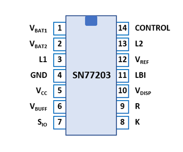
| Pin | IO | Function | Pin | IO | Function |
| 1 | V | VBAT1 (1.5 V In) | 14 | I | CONTROL (VDISP on/off) |
| 2 | V | VBAT2 (1.5 V In) | 13 | V | L2 (to GND) |
| 3 | V | L1 (to VBAT1) | 12 | V | VREF (C to GND) |
| 4 | V | GND | 11 | O | LBI (Low Battery Ind.) |
| 5 | V | VCC (+3.0 V Out) | 10 | V | VDISP (-4.0 V Out) |
| 6 | V | VBUFF (+3.0 V Out) | 9 | I | R (SI/O from TP0485) |
| 7 | IO | SI/O (Peripheral Bus) | 8 | O | K (SI/O to TP0485) |
If you have additions to the above datasheet please email: joerg@datamath.org.
© Sean Riddle and oerg Woerner, January 22, 2021. No reprints
without written permission.