DATAMATH CALCULATOR MUSEUM
|
|
DATAMATH CALCULATOR MUSEUM |
Characterization of Frontier Single-chip Calculator Circuits
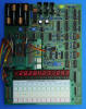
The DCM-50A Platform supports the Characterization of many Non-TI single-chip calculator circuits with up to 42-pin packages using the DCM-50A Playground DIL42 Adapter mounted on top of the DCM-50A PG Frame Carrier or the DCM-50A PG Digit Inverter Frame Carrier with the voltages VSS and VDD/VGG set to the appropriate level. The optional DCM-50A Playground Digilent I/O Extender supports Characterization and Reverse-engineering of Frontier single-chip calculator circuits.
The Characterization of the FR1001 is supported by using the DCM-50A Playground DIL42 Adapter mounted on top of the DCM-50A PG Digit Inverter Frame Carrier and the clock signals provided by the DCM-50A (PLAYGROUND) 2-Phase Clock Module.
 Device-under-Test:
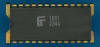
| • Package Markings Top:
FR 1001 73443 • Package Markings Bottom: • Donor Calculator: Unitrex 1200K (Type 47), November 1973 |
Keyboard: The Unitrex 1200K makes use of a keyboard assembly with 17 spring-loaded plastic keys pushing two fingers of stamped sheet-metal pieces soldered perpendicular on a single-sided phenolic PCB together with a 2-position sliding switch for the Constant Mode selection. The Decimal Point selection is preformed by simultaneously pressing the Decimal Point Key and a Number Key between 0 and 4. All switches are arranged in a 12*3 matrix connected to twelve digit-driver outputs D1-D12 and the key-matrix inputs KN (Numbers), KO (Operations). The [K] switch is connected with two diodes between the digit-driver outputs D2 and D4 and the key-matrix input KK (Constant).
Keyboard Matrix of the Unitrex 1200K (Type 47):
FR1001 | |||
| KN | KO | KK | |
| D1 | 2 | . | |
| D2 | 3 | [- K] | |
| D3 | += | ||
| D4 | 6 | [- K] | |
| D5 | |||
| D6 | 9 | −= | |
| D7 | 8 | ||
| D8 | 5 | ||
| D9 | 0 | C | |
| D10 | 1 | CE | |
| D11 | 4 | × | |
| D12 | 7 | ÷ | |
 Display:
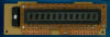
The Unitrex 1200K makes use of an unknown Panaplex-style display with three
9-pin Transistor modules connected with 12 high-voltage capacitors as level
shifters to the twelve Digit Outputs D1 to D12 of the FR1001 chip and two 9-pin
Transistor modules connected to the Segment Outputs SA to SG and SDP of the
FR1001 chip. Each of the five modules contains four PNP BJTs (Bipolar Junction
Transistors) with their Emitters connected to a common pin. The display is
operated with approximately +170 Volts. An additional discrete orange miniature
gas-discharge lamp
is used as minus sign for negative numbers.
Display:
The Unitrex 1200K makes use of an unknown Panaplex-style display with three
9-pin Transistor modules connected with 12 high-voltage capacitors as level
shifters to the twelve Digit Outputs D1 to D12 of the FR1001 chip and two 9-pin
Transistor modules connected to the Segment Outputs SA to SG and SDP of the
FR1001 chip. Each of the five modules contains four PNP BJTs (Bipolar Junction
Transistors) with their Emitters connected to a common pin. The display is
operated with approximately +170 Volts. An additional discrete orange miniature
gas-discharge lamp
is used as minus sign for negative numbers.
Display Layout:
| Unknown Panaplex-style plus Lamp |
 |
| The Segment drivers A-G and DP (Decimal Point) are connected to the unknown Panaplex-style display in the pictured way. | 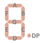 |
Display Fonts:
| Type | Calculator | Number Fonts | Decimal Separator |
Thousands Separator |
Entry Overflow |
Calculating Overflow |
Minus |
| FR1001 | Unitrex 1200K (Type 47) |
 |
 |
n.a. |
 |
|
 |
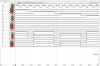
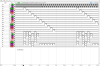 Display
scanning: The FR5001 single-chip calculator circuit is manufactured in a
PMOS process and its Digit Scanning Outputs are high-side PMOS transistors. For
easy interfacing to low-voltage VFDs
(Vacuum Fluorescent Displays) or high-voltage
gas-discharge displays, an
activated digit corresponds to a logical 0 or open output. All other,
non-activated digits have the PMOS transistors turned on. Please notice that the
the DCM-50A PG Digit Inverter Frame Carrier used to characterize the FR1001 chip
is inverting the Digit Outputs D1 to D12 and we labeled them therefore /D1 to
/D12 on the graphs.
Display
scanning: The FR5001 single-chip calculator circuit is manufactured in a
PMOS process and its Digit Scanning Outputs are high-side PMOS transistors. For
easy interfacing to low-voltage VFDs
(Vacuum Fluorescent Displays) or high-voltage
gas-discharge displays, an
activated digit corresponds to a logical 0 or open output. All other,
non-activated digits have the PMOS transistors turned on. Please notice that the
the DCM-50A PG Digit Inverter Frame Carrier used to characterize the FR1001 chip
is inverting the Digit Outputs D1 to D12 and we labeled them therefore /D1 to
/D12 on the graphs.
Display scanning is performed in D1 → D12 direction at a rate of about 310 Hz:
|
• State Time = 0.5 Clocks = 0.020 ms @ CK=25 kHz • Digit Time = 8 States = 0.160 ms @ CK=25 kHz • Scan Time = 20 Digit Times (D1 to D20 with D13 to D20 a dead cycle) = 3.20 ms @ CK=25 kHz |

If you have additions to the above article please email: joerg@datamath.org.
© Joerg Woerner, June 20, 2026. No reprints without written permission.