DATAMATH CALCULATOR MUSEUM
|
|
DATAMATH CALCULATOR MUSEUM |
Characterization of Single-chip Calculator Circuits - TMS1040 Product Family
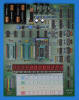
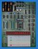
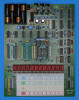
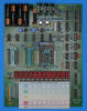
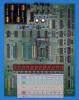
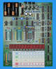
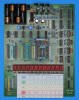
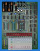
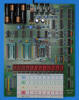
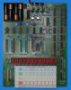
The DCM-50A Platform supports the Characterization of TMS1040 Devices in its rightmost TMS1000 Textool Test Socket with an additional TMS1040 Adapter and the voltages VSS set to 9.5V and VDD/VGG set to -5.5V.
 Device-under-Test:
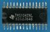
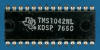
| • Package Markings Top: TMS1042NL, KDSΔ7638 • Package Markings Bottom: NONE • Donor Calculator: Canon LD-8Rs, October 1976 |
Keyboard: The Canon Palmtronic LD-8Rs and its siblings LD-8s and LD-8Ms make use of a keyboard with with conductive rubber switches arranged in an 7*4 matrix with the rows connected to the R0-R6 Outputs (Display Scan) and the columns connected to the K1-K8 Inputs (Keyboard Scan) of the TMS1042NL single-chip calculator circuit. R8 is jumpered for the LD-8Rs with a Diode directly to K1.
Keyboard Matrix of the Canon LD-8s Series:
| K1 | K2 | K4 | K8 | |
| R0 (D1) | 0 | 6 | = | RM (2) |
| R1 (D2) | 1 | 7 | ||
| R2 (D3) | 2 | 8 | M+= (2) | RCM (3) |
| R3 (D4) | 3 | 9 | M−= (2) | CI |
| R4 (D5) | 4 | . | %± | |
| R5 (D6) | 5 | √x (1) | CM (2) | C |
| R6 (D7) | − | + | ÷ | × |
| R7 (D8) | ||||
| R8 (D9) | [AM] (3) |
Notes: x(1) Implemented in TMS1042NL but not available on LD-8Rs, x(2) Implemented in TMS1042NL but only available on LS-8Ms, x(3) Implemented in TMS1042NL but only available on LD-8Rs. [AM] implemented with a hard-wired Diode in LD-8Rs only
![]() Display: The
Canon LD-8Rs makes use of a 9-digit Itron FG95D6 low-voltage Vacuum Fluorescent
Display (VFD) connected directly to the respective 9 R Outputs (Display Scan)
and 8 O Outputs (Segments) of the TMS1042NL and biased to approximately -30 Volts with its internal pull-down
resistors connected to VPP. We located in a LD-8s manufactured in May
1978 an Itron FG95F6 display while the LD-8Ms is using a similar Futaba 9-ST-11
display.
Display: The
Canon LD-8Rs makes use of a 9-digit Itron FG95D6 low-voltage Vacuum Fluorescent
Display (VFD) connected directly to the respective 9 R Outputs (Display Scan)
and 8 O Outputs (Segments) of the TMS1042NL and biased to approximately -30 Volts with its internal pull-down
resistors connected to VPP. We located in a LD-8s manufactured in May
1978 an Itron FG95F6 display while the LD-8Ms is using a similar Futaba 9-ST-11
display.
Display Layout:
| Itron FG95D6 |
|
|
The Output Decoder PLA of the TMS1042NL is programmed for 7-Segment displays with the following Output Assignments:
| TMS1042 Pin | 17 | 16 | 15 | 14 | 13 | 12 | 11 | 10 |
| TMS1042 Port | O0 | O1 | O2 | O3 | O4 | O5 | O6 | O7 |
| Segment | A | B | C | D | E | F | G | DP |
| The Segment drivers A-G and DP (Decimal Point) are connected to the Itron FG95D6 display in the pictured way. | 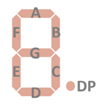 |
Display Fonts:
| Type | Calculator | Number Fonts | Decimal Separator |
Thousands Separator |
Entry Overflow |
Calculating Overflow |
Minus | Memory Indicator |
| TMS1042NL | Canon LD-8Rs | n.a. |
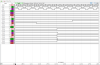
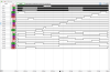 Scanning: Display and keyboard scanning is performed in R8 → R0 direction
followed by an RX State to display the Decimal Point at the desired position at a rate of about 220 Hz.
Blank Positions have a shorter Active Digit Time and longer Trailing Digit
Blanking Time:
Scanning: Display and keyboard scanning is performed in R8 → R0 direction
followed by an RX State to display the Decimal Point at the desired position at a rate of about 220 Hz.
Blank Positions have a shorter Active Digit Time and longer Trailing Digit
Blanking Time:
|
• Instruction Cycle Time
(ICT) = 6 Clocks = 0.02 ms @ CK=300 kHz • Leading Digit Blanking Time = 2 ICT = 0.04 ms • Active Digit Time R8 to R0 = 6 or 18 ICT = 0.12 ms or 0.36 ms • Trailing Digit Blanking = 14 or 2 ICT = 0.28 ms or 0.04 ms • Additional State RX State (Decimal Point) = 26 ICT = 0.52 ms • Display Cycle Time = 224 ICT = 4.48 ms |
 Device-under-Test:
| • Package Markings Top: TMS1042NL, KDSP 7650 • Package Markings Bottom: ⚫JP1042DS, SINGAPORE • Donor Calculator: Sharp EL-8117K, February 1977 |
Keyboard: The Sharp EL-8117K makes use of a keyboard with triangular snap-action dome switches (United States Patent 3,796,843 from March 12, 1974) arranged in an 7*4 matrix with the rows connected to the R0-R6 Outputs (Display Scan) and the columns connected to the K1-K8 Inputs (Keyboard Scan) of the TMS1042NL single-chip calculator circuit.
Keyboard Matrix of the Sharp EL-8117K:
| K1 | K2 | K4 | K8 | |
| R0 (D1) | 0 | 6 | = | |
| R1 (D2) | 1 | 7 | RCM | |
| R2 (D3) | 2 | 8 | M+ | |
| R3 (D4) | 3 | 9 | M− | |
| R4 (D5) | 4 | . | % | C/CE |
| R5 (D6) | 5 | √x | ||
| R6 (D7) | − | + | ÷ | × |
| R7 (D8) | ||||
| R8 (D9) |
![]() Display: The
Sharp EL-8117K makes use of a 9-digit Futaba 9-ST-12 low-voltage Vacuum Fluorescent
Display (VFD) connected directly to the respective 9 R Outputs (Display Scan)
and 8 O Outputs (Segments) of the TMS1042NL and biased to approximately -28 Volts with its internal pull-down
resistors connected to VPP.
Display: The
Sharp EL-8117K makes use of a 9-digit Futaba 9-ST-12 low-voltage Vacuum Fluorescent
Display (VFD) connected directly to the respective 9 R Outputs (Display Scan)
and 8 O Outputs (Segments) of the TMS1042NL and biased to approximately -28 Volts with its internal pull-down
resistors connected to VPP.
Display Layout:
| Futaba-9-ST-12 |
|
|
The Output Decoder PLA of the TMS1042NL is programmed for 7-Segment displays with the following Output Assignments:
| TMS1042 Pin | 17 | 16 | 15 | 14 | 13 | 12 | 11 | 10 |
| TMS1042 Port | O0 | O1 | O2 | O3 | O4 | O5 | O6 | O7 |
| Segment | A | B | C | D | E | F | G | DP |
| The Segment drivers A-G and DP (Decimal Point) are connected to the Futaba 9-ST-12 display in the pictured way. | |
Display Fonts:
| Type | Calculator | Number Fonts | Decimal Separator |
Thousands Separator |
Entry Overflow |
Calculating Overflow |
Minus | Memory Indicator |
| TMS1042NL | Sharp EL-8117K | n.a. |
|
|
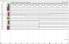
 Scanning: Display and keyboard scanning is performed in R8 → R0 direction
followed by an RX State to display the Decimal Point at the desired position at a rate of about 220 Hz.
Blank Positions have a shorter Active Digit Time and longer Trailing Digit
Blanking Time:
Scanning: Display and keyboard scanning is performed in R8 → R0 direction
followed by an RX State to display the Decimal Point at the desired position at a rate of about 220 Hz.
Blank Positions have a shorter Active Digit Time and longer Trailing Digit
Blanking Time:
|
• Instruction Cycle Time
(ICT) = 6 Clocks = 0.02 ms @ CK=300 kHz • Leading Digit Blanking Time = 2 ICT = 0.04 ms • Active Digit Time R8 to R0 = 6 or 18 ICT = 0.12 ms or 0.36 ms • Trailing Digit Blanking = 14 or 2 ICT = 0.28 ms or 0.04 ms • Additional State RX State (Decimal Point) = 26 ICT = 0.52 ms • Display Cycle Time = 224 ICT = 4.48 ms |
 Device-under-Test:
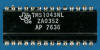
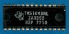
| • Package Markings Top: TMS1043NL,
ZA0352, AP 7636 • Package Markings Bottom: DP1043A, SINGAPORE • Donor Calculator: TI-2550 III, LTA 3776 |
Keyboard: The TI-2550 III makes use of a keyboard with snap-action dome switches arranged in an 7*4 matrix with the rows connected to the R0-R6 Outputs (Display Scan) and the columns connected to the K1-K8 Inputs (Keyboard Scan) of the TMS1043NL single-chip calculator circuit.
Keyboard Matrix of the TI-2550 III:
| K1 | K2 | K4 | K8 | |
| R0 (D1) | CE | 0 | . | = |
| R1 (D2) | 1 | 2 | 3 | + |
| R2 (D3) | 4 | 5 | 6 | − |
| R3 (D4) | 7 | 8 | 9 | × |
| R4 (D5) | C | +/− | % | ÷ |
| R5 (D6) | CM | MR | M− | M+ |
| R6 (D7) | RV | √x | x2 | 1/x |
| R7 (D8) | ||||
| R8 (D9) |
![]() Display: The TI-2550 III makes use of a 9-digit Itron
FG95B1 low-voltage Vacuum Fluorescent Display (VFD) connected directly to the
respective 9 R Outputs (Display Scan) and 8 O Outputs (Segments) of the
TMS1043NL and biased to approximately -30 Volts with its internal pull-down
resistors connected to VPP. Please notice that Texas Instruments designed the
calculator to accommodate the NEC LD8118L VFD, too. We refer these models as
TI-2550 III (Version 2).
Display: The TI-2550 III makes use of a 9-digit Itron
FG95B1 low-voltage Vacuum Fluorescent Display (VFD) connected directly to the
respective 9 R Outputs (Display Scan) and 8 O Outputs (Segments) of the
TMS1043NL and biased to approximately -30 Volts with its internal pull-down
resistors connected to VPP. Please notice that Texas Instruments designed the
calculator to accommodate the NEC LD8118L VFD, too. We refer these models as
TI-2550 III (Version 2).
Display Layout:
| Itron FG95B1 |
|
|
The Output Decoder PLA of the TMS1043NL is programmed for 7-Segment displays with the following Output Assignments:
| TMS1043 Pin | 17 | 16 | 15 | 14 | 13 | 12 | 11 | 10 |
| TMS1043 Port | O0 | O1 | O2 | O3 | O4 | O5 | O6 | O7 |
| Segment | A | B | C | D | E | F | G | DP |
| The Segment drivers A-G and DP (Decimal Point) are connected to the Itron FG95B1 display in the pictured way. | |
Display Fonts:
| Type | Calculator | Number Fonts | Decimal Separator |
Thousands Separator |
Entry Overflow |
Calculating Overflow |
Minus | Memory Indicator |
| TMS1043NL | TI-2550 III | n.a. |
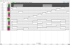
 Scanning: Display and keyboard scanning is performed in R8 → R0 direction at a rate of about 240 Hz
with one Blank State after R0 and R8 shorter than R7 to R1:
Scanning: Display and keyboard scanning is performed in R8 → R0 direction at a rate of about 240 Hz
with one Blank State after R0 and R8 shorter than R7 to R1:
|
• Instruction Cycle Time
(ICT) = 6 Clocks = 0.02 ms @ CK=300 kHz • Leading Digit Blanking Time = 2 ICT = 0.04 ms • Active Digit Time R8 = 14 ICT = 0.28 ms • Active Digit Time R7 to R0 = 18 ICT = 0.36 ms • Trailing Digit Blanking = 2 ICT = 0.04 ms • Blank State R0 → R8 = 13 ICT = 0.26 ms • Display Cycle Time = 207 ICT = 4.14 ms |
 Device-under-Test:
| • Package Markings Top: TMS1043NL,
ZA0352, BSP 7710 • Package Markings Bottom: DP1043BS, SINGAPORE • Donor Calculator: TI-2550 III, MTA 4077 |
Keyboard: The TI-2550 III makes use of a keyboard with snap-action dome switches arranged in an 7*4 matrix with the rows connected to the R0-R6 Outputs (Display Scan) and the columns connected to the K1-K8 Inputs (Keyboard Scan) of the TMS1043BNL single-chip calculator circuit.
Keyboard Matrix of the TI-2550 III:
| K1 | K2 | K4 | K8 | |
| R0 (D1) | CE | 0 | . | = |
| R1 (D2) | 1 | 2 | 3 | + |
| R2 (D3) | 4 | 5 | 6 | − |
| R3 (D4) | 7 | 8 | 9 | × |
| R4 (D5) | C | +/− | % | ÷ |
| R5 (D6) | CM | MR | M− | M+ |
| R6 (D7) | RV | √x | x2 | 1/x |
| R7 (D8) | ||||
| R8 (D9) |
![]() Display: The TI-2550 III makes use of a 9-digit
NEC LD8118L low-voltage Vacuum Fluorescent Display (VFD) connected directly to the
respective 9 R Outputs (Display Scan) and 8 O Outputs (Segments) of the
TMS1043BNL and biased to approximately -30 Volts with its internal pull-down
resistors connected to VPP. Please notice that Texas Instruments designed the
calculator to accommodate the Itron FG95B1 VFD, too. We refer these models as
TI-2550 III (Version 1).
Display: The TI-2550 III makes use of a 9-digit
NEC LD8118L low-voltage Vacuum Fluorescent Display (VFD) connected directly to the
respective 9 R Outputs (Display Scan) and 8 O Outputs (Segments) of the
TMS1043BNL and biased to approximately -30 Volts with its internal pull-down
resistors connected to VPP. Please notice that Texas Instruments designed the
calculator to accommodate the Itron FG95B1 VFD, too. We refer these models as
TI-2550 III (Version 1).
Display Layout:
| NEC LD8118L |
|
|
The Output Decoder PLA of the TMS1043BNL is programmed for 7-Segment displays with the following Output Assignments:
| TMS1043B Pin | 17 | 16 | 15 | 14 | 13 | 12 | 11 | 10 |
| TMS1043B Port | O0 | O1 | O2 | O3 | O4 | O5 | O6 | O7 |
| Segment | A | B | C | D | E | F | G | DP |
| The Segment drivers A-G and DP (Decimal Point) are connected to the NEC LD8118L display in the pictured way. | |
Display Fonts:
| Type | Calculator | Number Fonts | Decimal Separator |
Thousands Separator |
Entry Overflow |
Calculating Overflow |
Minus | Memory Indicator |
| TMS1043BNL | TI-2550 III | n.a. |
 Scanning: Display and keyboard scanning is performed in R8 → R0 direction at a rate of about 240 Hz
with one Blank State after R0 and R8 shorter than R7 to R1:
Scanning: Display and keyboard scanning is performed in R8 → R0 direction at a rate of about 240 Hz
with one Blank State after R0 and R8 shorter than R7 to R1:
|
• Instruction Cycle Time
(ICT) = 6 Clocks = 0.02 ms @ CK=300 kHz • Leading Digit Blanking Time = 2 ICT = 0.04 ms • Active Digit Time R8 = 14 ICT = 0.28 ms • Active Digit Time R7 to R0 = 18 ICT = 0.36 ms • Trailing Digit Blanking = 2 ICT = 0.04 ms • Blank State R0 → R8 = 13 ICT = 0.26 ms • Display Cycle Time = 207 ICT = 4.14 ms |
 Device-under-Test:
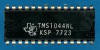
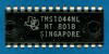
| • Package Markings Top: TMS1044NL,
KSP 7723 • Package Markings Bottom: ⚫JP1044S, SINGAPORE • Donor Calculator: Bohsei Model 1000, September 1977 |
Keyboard: The Bohsei Model 1000 makes use of a keyboard with triangular snap-action dome switches (United States Patent 3,796,843 from March 12, 1974) arranged in a 9*4 matrix with the rows connected to the R0-R8 Outputs (Display Scan) and the columns connected to the K2-K8 and the "virtual" K10 Inputs (Keyboard Scan) of the TMS1044NL single-chip calculator circuit.
Keyboard Matrix of the Bohsei Model 1000:
| K1 | K2 | K4 | K8 | V K10 | |
| R0 (D1) | 0 | 6 | |||
| R1 (D2) | 1 | 7 | = | ||
| R2 (D3) | 2 | 8 | MX | M− | |
| R3 (D4) | 3 | 9 | 1/x | M+ | |
| R4 (D5) | 4 | . | √x | ||
| R5 (D6) | 5 | PI | |||
| R6 (D7) | % | R/CM | |||
| R7 (D8) | − | + | ÷ | × | |
| R8 (D9) | C/CE |
Notes: K10 is a "virtual" 5th Keyboard Input line connected with two diodes to the K2 and K8 Keyboard Inputs of the TMS1044NL
![]() Display: The
Bohsei Model 1000 makes use of an 8-digit Itron DP84K low-voltage Vacuum Fluorescent Display (VFD) connected directly to the
respective 9 R Outputs (Display Scan) and 8 O Outputs (Segments) of the
TMS1044NL and biased to approximately -26 Volts with its internal and three
external (R6-100k Ohm, R7-100k Ohm, R8-12k Ohm) pull-down
resistors connected to VPP.
Display: The
Bohsei Model 1000 makes use of an 8-digit Itron DP84K low-voltage Vacuum Fluorescent Display (VFD) connected directly to the
respective 9 R Outputs (Display Scan) and 8 O Outputs (Segments) of the
TMS1044NL and biased to approximately -26 Volts with its internal and three
external (R6-100k Ohm, R7-100k Ohm, R8-12k Ohm) pull-down
resistors connected to VPP.
Display Layout:
| Itron DP84K |
|
|
The Output Decoder PLA of the TMS1044NL is programmed for 7-Segment displays with the following Output Assignments:
| TMS1044 Pin | 17 | 16 | 15 | 14 | 13 | 12 | 11 | 10 |
| TMS1044 Port | O0 | O1 | O2 | O3 | O4 | O5 | O6 | O7 |
| Segment | A | B | C | D | E | F | G | DP |
| The Segment drivers A-G and DP (Decimal Point) are connected to the Itron DP84K display in the pictured way. | |
Display Fonts:
| Type | Calculator | Number Fonts | Decimal Separator |
Thousands Separator |
Entry Overflow |
Calculating Overflow |
Minus | Memory Indicator |
| TMS1044NL | Bohsei 1000 |
|
n.a. |
 Scanning: Display and keyboard scanning is performed in R8 → R0 direction
followed by an RX State to display the Decimal Point at the desired position at a rate of about 240 Hz.
Blank Positions have a shorter Active Digit Time and longer Trailing Digit
Blanking Time:
Scanning: Display and keyboard scanning is performed in R8 → R0 direction
followed by an RX State to display the Decimal Point at the desired position at a rate of about 240 Hz.
Blank Positions have a shorter Active Digit Time and longer Trailing Digit
Blanking Time:
|
• Instruction Cycle Time
(ICT) = 6 Clocks = 0.02 ms @ CK=300 kHz • Leading Digit Blanking Time = 2 ICT = 0.04 ms • Active Digit Time R8 to R0 = 6 or 16 ICT = 0.12 ms or 0.32 ms • Trailing Digit Blanking = 12 or 2 ICT = 0.24 ms or 0.04 ms • Additional State RX State (Decimal Point) = 27 ICT = 0.54 ms • Display Cycle Time = 207 ICT = 4.14 ms |
 Device-under-Test:
| • Package Markings Top: TMS1044NL,
KSP 7723 • Package Markings Bottom: *JP1044S, SINGAPORE • Donor Calculator: Bohsei Model 1000, September 1977 • Explored Calculator: Privileg 858 MD, January 1977 |
Keyboard: The Privileg 858 MD makes use of a keyboard with with conductive rubber switches arranged in a 9*4 matrix with the rows connected to the R0-R8 Outputs (Display Scan) and the columns connected to the K2-K8 and the "virtual" K10 Inputs (Keyboard Scan) of the TMS1044NL single-chip calculator circuit.
Keyboard Matrix of the Privileg 858 MD:
| K1 | K2 | K4 | K8 | V K10 | |
| R0 (D1) | 0 | 6 | +/− | Δ% | |
| R1 (D2) | 1 | 7 | X-Y | = | |
| R2 (D3) | 2 | 8 | X-M | M− | |
| R3 (D4) | 3 | 9 | 1/x | M+ | |
| R4 (D5) | 4 | . | √x | ||
| R5 (D6) | 5 | PI | x2 | ||
| R6 (D7) | % | CM | RM | ||
| R7 (D8) | − | + | ÷ | × | |
| R8 (D9) | [ - ∑] | → | C/CE |
Notes: [y z] Sliding Switch Function, y Switch open, z Switch closed. K10 is a "virtual" 5th Keyboard Input line connected with two diodes to the K2 and K8 Keyboard Inputs of the TMS1044NL
Display: The Privileg 858 MD makes use of a 9-digit Futaba 9-ST-10 low-voltage Vacuum Fluorescent Display (VFD) connected directly to the respective 9 R Outputs (Display Scan) and 8 O Outputs (Segments) of the TMS1044NL and biased to approximately -28 Volts with its internal pull-down resistors connected to VPP.
Display Layout:
| Futaba 9-ST-10 |
|
|
The Output Decoder PLA of the TMS1044NL is programmed for 7-Segment displays with the following Output Assignments:
| TMS1044 Pin | 17 | 16 | 15 | 14 | 13 | 12 | 11 | 10 |
| TMS1044 Port | O0 | O1 | O2 | O3 | O4 | O5 | O6 | O7 |
| Segment | A | B | C | D | E | F | G | DP |
| The Segment drivers A-G and DP (Decimal Point) are connected to the Futaba 9-ST-10 display in the pictured way. | |
Display Fonts:
| Type | Calculator | Number Fonts | Decimal Separator |
Thousands Separator |
Entry Overflow |
Calculating Overflow |
Minus | Memory Indicator |
| TMS1044NL | Privileg 858 MD |
|
n.a. |
Scanning: Display and keyboard scanning is performed in R8 → R0 direction
followed by an RX State to display the Decimal Point at the desired position at a rate of about 240 Hz.
Blank Positions have a shorter Active Digit Time and longer Trailing Digit
Blanking Time:
|
• Instruction Cycle Time
(ICT) = 6 Clocks = 0.02 ms @ CK=300 kHz • Leading Digit Blanking Time = 2 ICT = 0.04 ms • Active Digit Time R8 to R0 = 6 or 16 ICT = 0.12 ms or 0.32 ms • Trailing Digit Blanking = 12 or 2 ICT = 0.24 ms or 0.04 ms • Additional State RX State (Decimal Point) = 27 ICT = 0.54 ms • Display Cycle Time = 207 ICT = 4.14 ms |
 Device-under-Test:
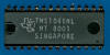
| • Package Markings Top: TMS1044NL,
MT 8018, SINGAPORE • Package Markings Bottom: NONE • Donor Calculator: Brinlock Model 806, June 1980 |
Keyboard: The Brinlock Model 806 makes use of a keyboard with triangular snap-action dome switches (United States Patent 3,796,843 from March 12, 1974) arranged in a 9*4 matrix with the rows connected to the R0-R8 Outputs (Display Scan) and the columns connected to the K2-K8 and the "virtual" K10 Inputs (Keyboard Scan) of the TMS1044NL single-chip calculator circuit.
Keyboard Matrix of the Brinlock Model 806:
| K1 | K2 | K4 | K8 | V K10 | |
| R0 (D1) | 0 | 6 | |||
| R1 (D2) | 1 | 7 | = | ||
| R2 (D3) | 2 | 8 | M− | ||
| R3 (D4) | 3 | 9 | M+ | ||
| R4 (D5) | 4 | . | √x | ||
| R5 (D6) | 5 | ||||
| R6 (D7) | % | CM | RM | ||
| R7 (D8) | − | + | ÷ | × | |
| R8 (D9) | C/CE |
Notes: K10 is a "virtual" 5th Keyboard Input line connected with two diodes to the K2 and K8 Keyboard Inputs of the TMS1044NL
![]() Display: The
Brinlock Model 806 makes use of a 9-digit Futaba 9-ST-11 low-voltage Vacuum Fluorescent Display (VFD) connected directly to the
respective 9 R Outputs (Display Scan) and 8 O Outputs (Segments) of the
TMS1044NL and biased to approximately -28 Volts with its internal pull-down
resistors connected to VPP.
Display: The
Brinlock Model 806 makes use of a 9-digit Futaba 9-ST-11 low-voltage Vacuum Fluorescent Display (VFD) connected directly to the
respective 9 R Outputs (Display Scan) and 8 O Outputs (Segments) of the
TMS1044NL and biased to approximately -28 Volts with its internal pull-down
resistors connected to VPP.
Display Layout:
| Futaba 9-ST-11 |
|
|
The Output Decoder PLA of the TMS1044NL is programmed for 7-Segment displays with the following Output Assignments:
| TMS1044 Pin | 17 | 16 | 15 | 14 | 13 | 12 | 11 | 10 |
| TMS1044 Port | O0 | O1 | O2 | O3 | O4 | O5 | O6 | O7 |
| Segment | A | B | C | D | E | F | G | DP |
| The Segment drivers A-G and DP (Decimal Point) are connected to the Futaba 9-ST-11 display in the pictured way. | |
Display Fonts:
| Type | Calculator | Number Fonts | Decimal Separator |
Thousands Separator |
Entry Overflow |
Calculating Overflow |
Minus | Memory Indicator |
| TMS1044NL | Brinlock 806 |
|
n.a. |
Scanning: Display and keyboard scanning is performed in R8 → R0 direction
followed by an RX State to display the Decimal Point at the desired position at a rate of about 240 Hz.
Blank Positions have a shorter Active Digit Time and longer Trailing Digit
Blanking Time:
|
• Instruction Cycle Time
(ICT) = 6 Clocks = 0.02 ms @ CK=300 kHz • Leading Digit Blanking Time = 2 ICT = 0.04 ms • Active Digit Time R8 to R0 = 6 or 16 ICT = 0.12 ms or 0.32 ms • Trailing Digit Blanking = 12 or 2 ICT = 0.24 ms or 0.04 ms • Additional State RX State (Decimal Point) = 27 ICT = 0.54 ms • Display Cycle Time = 207 ICT = 4.14 ms |
 Device-under-Test:
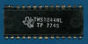
| • Package Markings Top: TMS1044NL,
TP 7745 • Package Markings Bottom: JP1044T, SINGAPORE • Donor Calculator: Unisonic Model 1040-1, December 1977 |
Keyboard: The Unisonic Model 1040-1 makes use of a keyboard with conductive rubber switches arranged in a 9*4 matrix with the rows connected to the R0-R8 Outputs (Display Scan) and the columns connected to the K2-K8 and the "virtual" K10 Inputs (Keyboard Scan) of the TMS1044NL single-chip calculator circuit.
Keyboard Matrix of the Unisonic Model 1040-1:
| K1 | K2 | K4 | K8 | V K10 | |
| R0 (D1) | 0 | 6 | +/− | GPM | |
| R1 (D2) | 1 | 7 | EX | = | |
| R2 (D3) | 2 | 8 | M− | ||
| R3 (D4) | 3 | 9 | M+ | ||
| R4 (D5) | 4 | . | √x | ||
| R5 (D6) | 5 | ||||
| R6 (D7) | % | CM | RM | ||
| R7 (D8) | − | + | ÷ | × | |
| R8 (D9) | CE | C |
Notes: K10 is a "virtual" 5th Keyboard Input line connected with two diodes to the K2 and K8 Keyboard Inputs of the TMS1044NL
![]() Display: The
Unisonic Model 1040-1 makes use of a 9-digit Futaba 9-ST-08A low-voltage Vacuum Fluorescent Display (VFD) connected directly to the
respective 9 R Outputs (Display Scan) and 8 O Outputs (Segments) of the
TMS1044NL and biased to approximately -27 Volts with its internal pull-down
resistors connected to VPP.
Display: The
Unisonic Model 1040-1 makes use of a 9-digit Futaba 9-ST-08A low-voltage Vacuum Fluorescent Display (VFD) connected directly to the
respective 9 R Outputs (Display Scan) and 8 O Outputs (Segments) of the
TMS1044NL and biased to approximately -27 Volts with its internal pull-down
resistors connected to VPP.
Display Layout:
| Futaba 9-ST-08A |
|
|
The Output Decoder PLA of the TMS1044NL is programmed for 7-Segment displays with the following Output Assignments:
| TMS1044 Pin | 17 | 16 | 15 | 14 | 13 | 12 | 11 | 10 |
| TMS1044 Port | O0 | O1 | O2 | O3 | O4 | O5 | O6 | O7 |
| Segment | A | B | C | D | E | F | G | DP |
| The Segment drivers A-G and DP (Decimal Point) are connected to the Futaba 9-ST-08A display in the pictured way. | |
Display Fonts:
| Type | Calculator | Number Fonts | Decimal Separator |
Thousands Separator |
Entry Overflow |
Calculating Overflow |
Minus | Memory Indicator |
| TMS1044NL | Unisonic 1040-1 |
|
n.a. |
 Scanning: Display and keyboard scanning is performed in R8 → R0 direction
followed by an RX State to display the Decimal Point at the desired position at a rate of about 240 Hz.
Blank Positions have a shorter Active Digit Time and longer Trailing Digit
Blanking Time:
Scanning: Display and keyboard scanning is performed in R8 → R0 direction
followed by an RX State to display the Decimal Point at the desired position at a rate of about 240 Hz.
Blank Positions have a shorter Active Digit Time and longer Trailing Digit
Blanking Time:
|
• Instruction Cycle Time
(ICT) = 6 Clocks = 0.02 ms @ CK=300 kHz • Leading Digit Blanking Time = 2 ICT = 0.04 ms • Active Digit Time R8 to R0 = 6 or 16 ICT = 0.12 ms or 0.32 ms • Trailing Digit Blanking = 12 or 2 ICT = 0.24 ms or 0.04 ms • Additional State RX State (Decimal Point) = 27 ICT = 0.54 ms • Display Cycle Time = 207 ICT = 4.14 ms |
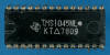
 Device-under-Test:
| • Package Markings Top: TMS1045NL,
KSΔ7723 • Package Markings Bottom: NONE • Donor Calculator: Canon F-31, June 1977 |
Keyboard: The Canon F-31 makes use of a keyboard with conductive rubber switches arranged in a 9*4 matrix with the rows connected to the R0-R8 Outputs (Display Scan) and the columns connected to the K2-K8 and the "virtual" K10 Inputs (Keyboard Scan) of the TMS1045NL single-chip calculator circuit. The [+ - 2 - 0 - F] sliding switch is connected between the R1, R2, and R0 Outputs and K1 Input. R7 is jumpered with a Diode directly to K1.
Keyboard Matrix of the Canon F-31:
| K1 | K2 | K4 | K8 | V K10 | |
| R0 (D1) | [+20F] | 0 | 6 | SC | M+ |
| R1 (D2) | [+20F] | 1 | 7 | RV | |
| R2 (D3) | [+20F] | 2 | 8 | ||
| R3 (D4) | 3 | 9 | 1/x | ( | |
| R4 (D5) | 4 | . | √x | ) | |
| R5 (D6) | 5 | PI | x2 | = | |
| R6 (D7) | %± | CM | RM | ||
| R7 (D8) | [Diode] | − | + | ÷ | × |
| R8 (D9) | → | CI/C |
Notes: [y z] Sliding Switch Function, y Switch open, z Switch closed. K10 is a "virtual" 5th Keyboard Input line connected with two diodes to the K2 and K8 Keyboard Inputs of the TMS1045NL
![]() Display: The
Canon F-31 makes use of a 9-digit Futaba 9-ST-11 low-voltage Vacuum Fluorescent Display (VFD) connected directly to the
respective 9 R Outputs (Display Scan) and 8 O Outputs (Segments) of the
TMS1045NL and biased to approximately -30 Volts with its internal pull-down
resistors connected to VPP.
Display: The
Canon F-31 makes use of a 9-digit Futaba 9-ST-11 low-voltage Vacuum Fluorescent Display (VFD) connected directly to the
respective 9 R Outputs (Display Scan) and 8 O Outputs (Segments) of the
TMS1045NL and biased to approximately -30 Volts with its internal pull-down
resistors connected to VPP.
Display Layout:
| Futaba 9-ST-11 |
|
|
The Output Decoder PLA of the TMS1045NL is programmed for 7-Segment displays with the following Output Assignments:
| TMS1045 Pin | 17 | 16 | 15 | 14 | 13 | 12 | 11 | 10 |
| TMS1045 Port | O0 | O1 | O2 | O3 | O4 | O5 | O6 | O7 |
| Segment | A | B | C | D | E | F | G | DP |
| The Segment drivers A-G and DP (Decimal Point) are connected to the Futaba 9-ST-11 display in the pictured way. | |
Display Fonts:
| Type | Calculator | Number Fonts | Decimal Separator |
Thousands Separator |
Entry Overflow |
Calculating Overflow |
Minus | Memory Indicator |
| TMS1045NL | Canon F-31 |
|
n.a. |
Scanning: Display and keyboard scanning is performed in R8 → R0 direction
followed by an RX State to display the Decimal Point at the desired position at a rate of about 240 Hz.
Blank Positions have a shorter Active Digit Time and longer Trailing Digit
Blanking Time:
|
• Instruction Cycle Time
(ICT) = 6 Clocks = 0.02 ms @ CK=300 kHz • Leading Digit Blanking Time = 2 ICT = 0.04 ms • Active Digit Time R8 to R0 = 6 or 16 ICT = 0.12 ms or 0.32 ms • Trailing Digit Blanking = 12 or 2 ICT = 0.24 ms or 0.04 ms • Additional State RX State (Decimal Point) = 27 ICT = 0.54 ms • Display Cycle Time = 207 ICT = 4.14 ms |
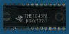
 Device-under-Test:
| • Package Markings Top: TMS1045NL⚫,
KTΔ7809 • Package Markings Bottom: NONE • Donor Calculator: Canon Canola L813, May 1978 |
Keyboard: The Canon Canola L813 makes use of a keyboard with conductive rubber switches arranged in a 9*4 matrix with the rows connected to the R0-R8 Outputs (Display Scan) and the columns connected to the K2-K8 and the "virtual" K10 Inputs (Keyboard Scan) of the TMS1045NL single-chip calculator circuit. The [+ - 4 - 2 - 0 - F] sliding switch is connected between the R1, R2, and R0 Outputs and K1 Input and the [ - AM] sliding switch is connected between R8 and K1. R7 is jumpered with a Diode directly to K1.
Keyboard Matrix of the Canon Canola L813:
| K1 | K2 | K4 | K8 | V K10 | |
| R0 (D1) | [+420F] | 0 | 6 | +/− | |
| R1 (D2) | [+420F] | 1 | 7 | ||
| R2 (D3) | [+420F] | 2 | 8 | ||
| R3 (D4) | 3 | 9 | |||
| R4 (D5) | [+420F] | 4 | . | ||
| R5 (D6) | 5 | = | |||
| R6 (D7) | %± | CM | RM | ||
| R7 (D8) | [Diode] | − | + | ÷ | × |
| R8 (D9) | [ - AM] | CI | C |
Notes: [y z] Sliding Switch Function, y Switch open, z Switch closed. K10 is a "virtual" 5th Keyboard Input line connected with two diodes to the K2 and K8 Keyboard Inputs of the TMS1045NL
![]() Display: The
Canon Canola L813 makes use of a 9-digit Futaba 9-BT-18A low-voltage Vacuum Fluorescent Display (VFD) connected directly to the
respective 9 R Outputs (Display Scan) and 8 O Outputs (Segments) of the
TMS1045NL and biased to approximately -32 Volts with its internal pull-down
resistors connected to VPP.
Display: The
Canon Canola L813 makes use of a 9-digit Futaba 9-BT-18A low-voltage Vacuum Fluorescent Display (VFD) connected directly to the
respective 9 R Outputs (Display Scan) and 8 O Outputs (Segments) of the
TMS1045NL and biased to approximately -32 Volts with its internal pull-down
resistors connected to VPP.
Display Layout:
| Futaba 9-BT-18A |
|
|
The Output Decoder PLA of the TMS1045NL is programmed for 7-Segment displays with the following Output Assignments:
| TMS1045 Pin | 17 | 16 | 15 | 14 | 13 | 12 | 11 | 10 |
| TMS1045 Port | O0 | O1 | O2 | O3 | O4 | O5 | O6 | O7 |
| Segment | A | B | C | D | E | F | G | DP |
| The Segment drivers A-G and DP (Decimal Point) are connected to the Futaba 9-BT-18A display in the pictured way. The additional Comma and Thousands Indicators are not connected. |  |
Display Fonts:
| Type | Calculator | Number Fonts | Decimal Separator |
Thousands Separator |
Entry Overflow |
Calculating Overflow |
Minus | Memory Indicator |
| TMS1045NL | Canon L813 |
|
n.a. |
 Scanning: Display and keyboard scanning is performed in R8 → R0 direction
followed by an RX State to display the Decimal Point at the desired position at a rate of about 240 Hz.
Blank Positions have a shorter Active Digit Time and longer Trailing Digit
Blanking Time:
Scanning: Display and keyboard scanning is performed in R8 → R0 direction
followed by an RX State to display the Decimal Point at the desired position at a rate of about 240 Hz.
Blank Positions have a shorter Active Digit Time and longer Trailing Digit
Blanking Time:
|
• Instruction Cycle Time
(ICT) = 6 Clocks = 0.02 ms @ CK=300 kHz • Leading Digit Blanking Time = 2 ICT = 0.04 ms • Active Digit Time R8 to R0 = 6 or 16 ICT = 0.12 ms or 0.32 ms • Trailing Digit Blanking = 12 or 2 ICT = 0.24 ms or 0.04 ms • Additional State RX State (Decimal Point) = 27 ICT = 0.54 ms • Display Cycle Time = 207 ICT = 4.14 ms |
 Device-under-Test:
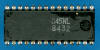
| • Package Markings Top: TMS1045NL,
___TΔ8432 • Package Markings Bottom: NONE • Donor Calculator: Canon Canola L813 II, August 1984 |
Keyboard: The Canon Canola L813 II makes use of a keyboard with conductive rubber switches arranged in a 9*4 matrix with the rows connected to the R0-R8 Outputs (Display Scan) and the columns connected to the K2-K8 and the "virtual" K10 Inputs (Keyboard Scan) of the TMS1045NL single-chip calculator circuit. The [+ - 4 - 2 - 0 - F] sliding switch is connected between the R1, R2, and R0 Outputs and K1 Input and the [ - AM] sliding switch is connected between R8 and K1. R7 is jumpered with a Diode directly to K1.
Keyboard Matrix of the Canon Canola L813 II:
| K1 | K2 | K4 | K8 | V K10 | |
| R0 (D1) | [+420F] | 0 | 6 | ||
| R1 (D2) | [+420F] | 1 | 7 | M−= | |
| R2 (D3) | [+420F] | 2 | 8 | M+= | |
| R3 (D4) | 3 | 9 | |||
| R4 (D5) | [+420F] | 4 | . | ||
| R5 (D6) | 5 | = | |||
| R6 (D7) | %± | RM/CM | |||
| R7 (D8) | [Diode] | − | + | ÷ | × |
| R8 (D9) | [ - AM] | CI | C |
Notes: [y z] Sliding Switch Function, y Switch open, z Switch closed. K10 is a "virtual" 5th Keyboard Input line connected with two diodes to the K2 and K8 Keyboard Inputs of the TMS1045NL
![]() Display: The
Canon Canola L813 II makes use of a 9-digit Futaba 9-BT-18A low-voltage Vacuum Fluorescent Display (VFD) connected directly to the
respective 9 R Outputs (Display Scan) and 8 O Outputs (Segments) of the
TMS1045NL and biased to approximately -31 Volts with its internal pull-down
resistors connected to VPP.
Display: The
Canon Canola L813 II makes use of a 9-digit Futaba 9-BT-18A low-voltage Vacuum Fluorescent Display (VFD) connected directly to the
respective 9 R Outputs (Display Scan) and 8 O Outputs (Segments) of the
TMS1045NL and biased to approximately -31 Volts with its internal pull-down
resistors connected to VPP.
Display Layout:
| Futaba 9-BT-18A |
|
|
The Output Decoder PLA of the TMS1045NL is programmed for 7-Segment displays with the following Output Assignments:
| TMS1045 Pin | 17 | 16 | 15 | 14 | 13 | 12 | 11 | 10 |
| TMS1045 Port | O0 | O1 | O2 | O3 | O4 | O5 | O6 | O7 |
| Segment | A | B | C | D | E | F | G | DP |
| The Segment drivers A-G and DP (Decimal Point) are connected to the Futaba 9-BT-18A display in the pictured way. The additional Comma and Thousands Indicators are not connected. | |
Display Fonts:
| Type | Calculator | Number Fonts | Decimal Separator |
Thousands Separator |
Entry Overflow |
Calculating Overflow |
Minus | Memory Indicator |
| TMS1045NL | Canon L813 II |
|
n.a. |
 Scanning: Display and keyboard scanning is performed in R8 → R0 direction
followed by an RX State to display the Decimal Point at the desired position at a rate of about 240 Hz.
Blank Positions have a shorter Active Digit Time and longer Trailing Digit
Blanking Time:
Scanning: Display and keyboard scanning is performed in R8 → R0 direction
followed by an RX State to display the Decimal Point at the desired position at a rate of about 240 Hz.
Blank Positions have a shorter Active Digit Time and longer Trailing Digit
Blanking Time:
|
• Instruction Cycle Time
(ICT) = 6 Clocks = 0.02 ms @ CK=300 kHz • Leading Digit Blanking Time = 2 ICT = 0.04 ms • Active Digit Time R8 to R0 = 6 or 16 ICT = 0.12 ms or 0.32 ms • Trailing Digit Blanking = 12 or 2 ICT = 0.24 ms or 0.04 ms • Additional State RX State (Decimal Point) = 27 ICT = 0.54 ms • Display Cycle Time = 207 ICT = 4.14 ms |

 Device-under-Test:
| • Package Markings Top: TMS1045NL,
MT 8001, SINGAPORE • Package Markings Bottom: NONE • Donor Calculator: Toshiba BC-8111B, January 1980 |
Keyboard: The Toshiba BC-8111B makes use of a keyboard with conductive rubber switches arranged in a 9*4 matrix with the rows connected to the R0-R8 Outputs (Display Scan) and the columns connected to the K2-K8 and the "virtual" K10 Inputs (Keyboard Scan) of the TMS1045NL single-chip calculator circuit.
Keyboard Matrix of the Toshiba BC-8111B and its siblings BC-8018B and BC-8112SL:
| K1 | K2 | K4 | K8 | V K10 | |
| R0 (D1) | 0 | 6 | |||
| R1 (D2) | 1 | 7 | M− (1) | ||
| R2 (D3) | 2 | 8 | M+ (1) | ||
| R3 (D4) | 3 | 9 | 1/x (2) | ( (2) | |
| R4 (D5) | 4 | . | √x | ) (2) | |
| R5 (D6) | 5 | PI | x2 (2) | = | |
| R6 (D7) | % | CM (1) | RM (1) | ||
| R7 (D8) | − | + | ÷ | × | |
| R8 (D9) | C/CE |
Notes: x(1) Implemented in TMS1045NL but not available on BC-8018B, x(2) Implemented in TMS1045NL but only available on BC-8111B, BC-8112SL and BC-8112SR. [y z] Sliding Switch Function, y Switch open, z Switch closed. K10 is a "virtual" 5th Keyboard Input line connected with two diodes to the K2 and K8 Keyboard Inputs of the TMS1045NL
![]() Display: The
Toshiba BC-8111B makes use of a 9-digit Futaba 9-ST-08A low-voltage Vacuum Fluorescent Display (VFD) connected directly to the
respective 9 R Outputs (Display Scan) and 8 O Outputs (Segments) of the
TMS1045NL and biased to approximately -27 Volts with its internal pull-down
resistors connected to VPP.
Display: The
Toshiba BC-8111B makes use of a 9-digit Futaba 9-ST-08A low-voltage Vacuum Fluorescent Display (VFD) connected directly to the
respective 9 R Outputs (Display Scan) and 8 O Outputs (Segments) of the
TMS1045NL and biased to approximately -27 Volts with its internal pull-down
resistors connected to VPP.
Display Layout:
| Futaba 9-ST-08A |
|
|
The Output Decoder PLA of the TMS1045NL is programmed for 7-Segment displays with the following Output Assignments:
| TMS1045 Pin | 17 | 16 | 15 | 14 | 13 | 12 | 11 | 10 |
| TMS1045 Port | O0 | O1 | O2 | O3 | O4 | O5 | O6 | O7 |
| Segment | A | B | C | D | E | F | G | DP |
| The Segment drivers A-G and DP (Decimal Point) are connected to the Futaba 9-ST-08A display in the pictured way. | |
Display Fonts:
| Type | Calculator | Number Fonts | Decimal Separator |
Thousands Separator |
Entry Overflow |
Calculating Overflow |
Minus | Memory Indicator |
| TMS1045NL | Toshiba BC-8111B |
|
n.a. |
Scanning: Display and keyboard scanning is performed in R8 → R0 direction
followed by an RX State to display the Decimal Point at the desired position at a rate of about 240 Hz.
Blank Positions have a shorter Active Digit Time and longer Trailing Digit
Blanking Time:
|
• Instruction Cycle Time
(ICT) = 6 Clocks = 0.02 ms @ CK=300 kHz • Leading Digit Blanking Time = 2 ICT = 0.04 ms • Active Digit Time R8 to R0 = 6 or 16 ICT = 0.12 ms or 0.32 ms • Trailing Digit Blanking = 12 or 2 ICT = 0.24 ms or 0.04 ms • Additional State RX State (Decimal Point) = 27 ICT = 0.54 ms • Display Cycle Time = 207 ICT = 4.14 ms |
If you have additions to the above article please email: joerg@datamath.org.
© Joerg Woerner, January 7, 2023. No reprints without written permission.